Parameters, Parameters –31 – Altera DDR SDRAM Controller User Manual
Page 67
Chapter 3: Functional Description
3–31
Parameters
© March 2009
Altera Corporation
DDR and DDR2 SDRAM Controller Compiler User Guide
Parameters
The parameters can be set only in IP Toolbench (refer to
Controller Walkthrough” on page 2–9
shows the global parameters.
clk_to_sdram
Output
Clock for the memory device.
clk_to_sdram_n
Output
Inverted clock for the memory device.
ddr_a[]
Output
Memory address bus.
ddr_ba[]
Output
Memory bank address bus.
ddr_cas_n
Output
Memory column address strobe signal.
ddr_cke[]
Output
Memory clock enable signals.
ddr_cs_n[]
Output
Memory chip select signals.
ddr_dm[]
Output
Memory data mask signal, which masks individual bytes during writes.
ddr_odt
Output
Memory on-die termination control signal (DDR2 SDRAM only).
ddr_ras_n
Output
Memory row address strobe signal.
ddr_we_n
Output
Memory write enable signal.
Note to
(1) You can change the ddr_ signal name prefix in IP Toolbench.
Table 3–9. DDR & DDR2 SDRAM Interface Signals (Part 2 of 2)
(Note 1)
Signal Name
Direction
Description
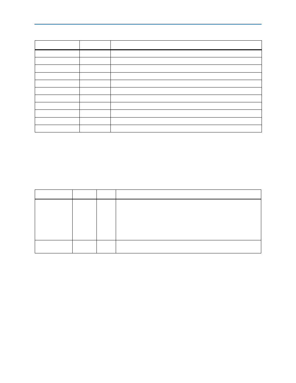
Table 3–10. Global Parameters
Parameter
Value
Units
Description
Presets
Part
number or
custom
—
A part number for a particular memory device, module, or the name of an
Altera development board. Choosing an entry other than Custom sets many of
the parameters in the wizard to the correct value for the specified part. If any
such parameter is changed to a value that is not supported by the specified
device, the preset automatically changes to custom. You can add your own
devices or boards to this list by editing the memory_types.dat file in the
\constraints directory.
Clock speed
> 75
MHz
The clock frequency used by the memory controller. Because the controller
uses double data rate, the data rate is twice the clock frequency.
Note to
:
(1) Depends on the FPGA and the memory device that you choose.