Note 1) – Altera DDR SDRAM Controller User Manual
Page 48
3–12
Chapter 3: Functional Description
Device-Level Description
DDR and DDR2 SDRAM Controller Compiler User Guide
© March 2009
Altera Corporation
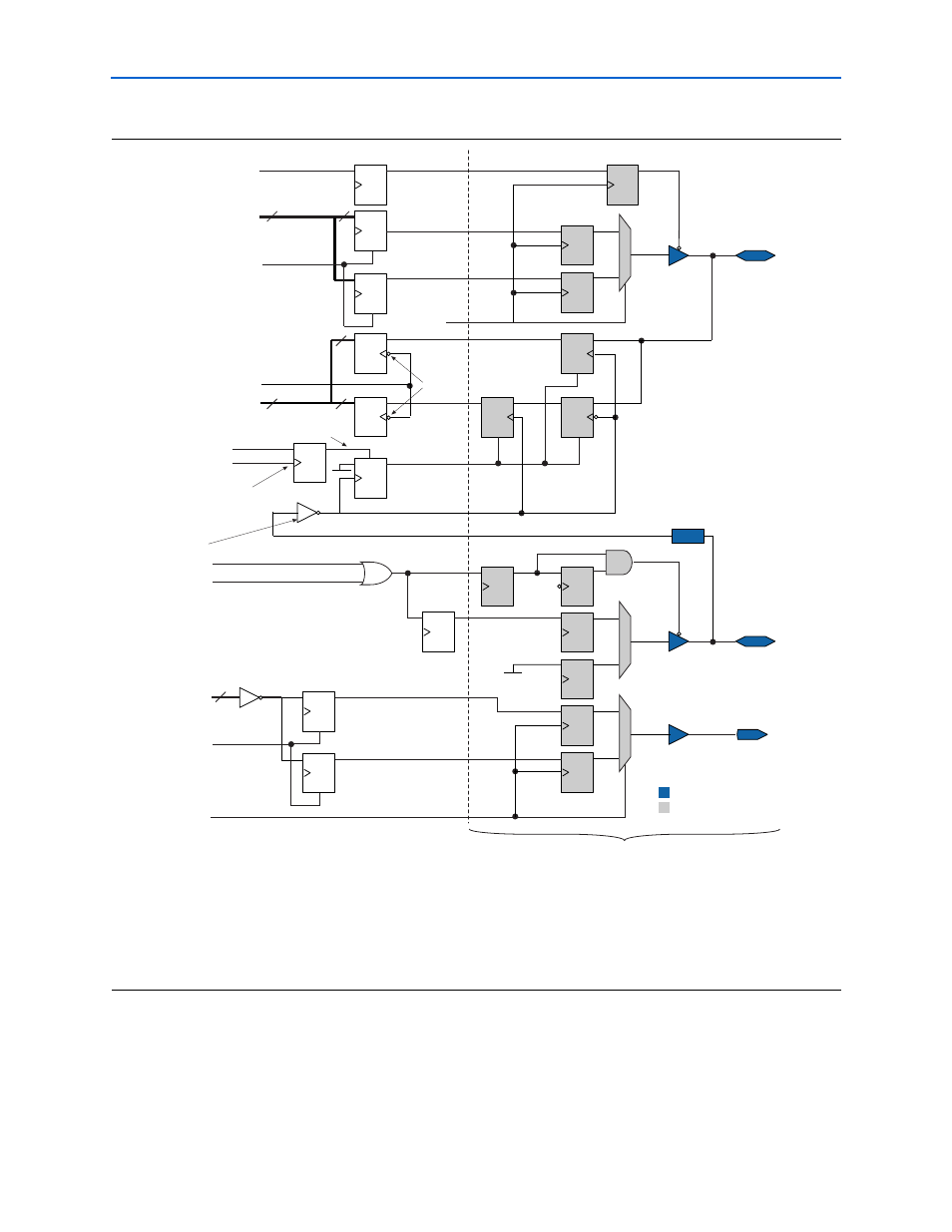
Figure 3–7. Cyclone DQS Group Block Diagram
Notes to
(1) This figure shows the logic for one dq output only. A complete byte group consists of eight times the DQ logic with the DQS and DM logic.
(2) All clocks are clk, unless marked otherwise.
(3) Each DQS requires a global clock resource. Invert combout of the ALTDDIO_BIDIR megafunction for the DQS pin before feeding in to inclock
of the ALTDDIO_BIDIR megafunction for the DQ pin.
(4) The optional inverters are controlled by the resynchronization edge and postamble edge settings on the Manual Timing tab, refer to
D
Q
D
w
rite_clk
altddio Megaf
u
nctions
d
q
s
dm
(Note 3)
d
q
s_oe
1
Delay
Ao
Bo
DQS_A
OE
B
OE
Programma
b
le
Delay
Q
0
1
D
Q
D
Q
0
1
D
Q
D
Q
Q
Q
D
D
b
e
doing_
w
r
d
q
s_
bu
rst
Q
D
2
Q
D
Q
D
Q
D
Q
D
Q
D
Q
D
Q
D
D
Q
Q
Q
D
Q
D
D
Q
D
Q
w
data
d
q
w
rite_clk
doing_
w
r
rdata
d
q
_ena
b
le_reset
postam
b
le_clk
resynched_data
d
q
_ena
b
le
d
q
_capt
u
re_clk
resynch_clk
d
q
_oe
16
DQ_A
OE
Ao
C
A
B
Bo
0
1
16
8
8
8
D
EN
EN
EN
EN
EN
doing_
w
r
EN
EN
w
data_valid
Preset (asynchronous)
I
I
I
IOEs
FPGA LEs
Optional Inverter (Note 4)
Optional Inverters (Note 4)