Avoiding back-driving problems, Routing considerations, Emi / esd protection – Kontron COMe Starterkit Eval T2 User Manual
Page 86: R 2.9.3 'avoiding back-driving problems, 86 below, Com express interfaces
COM Express Interfaces
2.9.3.
Avoiding Back-driving Problems
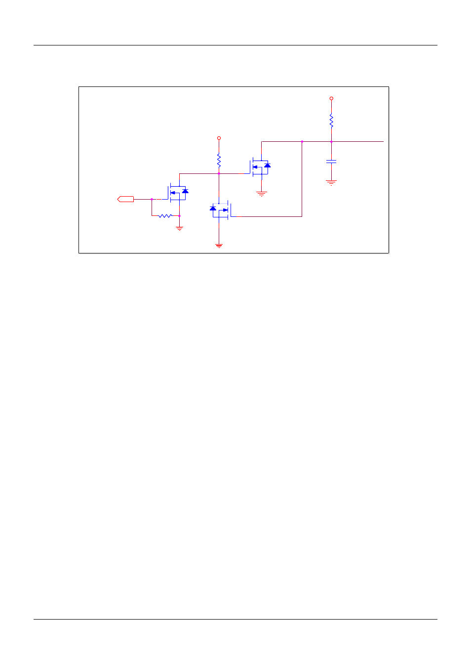
Figure 32:
Avoiding Back-driving
Back driving of power from a USB device to power rails on the Module can occur in some
designs. It is recommended that USB power not be enabled until the Module's standby power
rail (and therefore USB host power) is active. The COM Express standard does not provide a
signal from the Module to the Carrier indicating the chipset standby rail is up. This reference
schematic takes advantage of the USB_0_1_OC# pin as an indication of USB Host power. This
pin which is typically pulled up on the Module to the correct standby rail, may be used as shown
here to enable USB power. The FETs Q1, Q2 and Q3 form a latch and ensure that in case of an
over-current event no toggling situation will occur. To use this circuit do not install R43 in Figure
31: USB 3.0 Example Schematic and put instead the schematic in Figure 32: Avoiding Back-
driving. There may be other circuit implementations that perform the same functionality.
2.9.4.
Routing Considerations
Route USB data signals as differential pairs, with a 90-Ω differential impedance and a 45-Ω,
single-ended impedance. Route USB SuperSpeed signals as differential pairs, with an 85-Ω
differential impedance and a 50-Ω, single-ended impedance. Ideally, a USB pair is routed on a
single layer adjacent to a ground plane.
USB pairs should not cross plane splits. Keep layer transitions to a minimum. Reference USB
pairs to a power plane if necessary. The power plane should be well-bypassed. Section 6.5.3
'USB 3.0 Trace Routing Guidelines' on page 184 summarizes routing rules for SuperSpeed
signals. Section 6.5.2 'USB Trace Routing Guidelines' on page 183 below summarizes routing
rules for USB data signals.
2.9.4.1.
EMI / ESD Protection
To improve the EMI behavior of the USB interface, a design should include common mode
chokes, which have to be placed as close as possible to the USB connector signal pins.
Common mode chokes can provide required noise attenuation but they also distort the signal
quality of FullSpeed, HighSpeed and SuperSpeed signaling. Therefore, common mode chokes
should be chosen carefully to meet the requirements of the EMI noise filtering while retaining the
integrity of the USB signals on the Carrier Board design.
To protect the USB host interface of the Module from over-voltage caused by electrostatic
discharge (ESD) and electrical fast transients (EFT), low capacitance steering diodes and
transient voltage suppression diodes have to be implemented on the Carrier Board design. In
Figure 31: USB 3.0 Example Schematic on page 84 above, this is implemented by using Ultra-
Low capacitance ESD diode arrays from Infineon. (http://www.infineon.com).
PICMG
®
COM Express
®
Carrier Board Design Guide
Rev. 2.0 / December 6, 2013
86/218
2
1
3
R30
511k
USB_0_1_O C#
R32
10k
Q 1
BSS138W
DNI
V5.0_USB
CEX
2
1
3
Q 3
BSS138W
2
1
3
Q 2
BSS138W
C5
1µ
5V
R39
10k
V5.0_USB
ENABLE_VBUS