Figure 2 – Kontron COMe Starterkit Eval T2 User Manual
Page 17
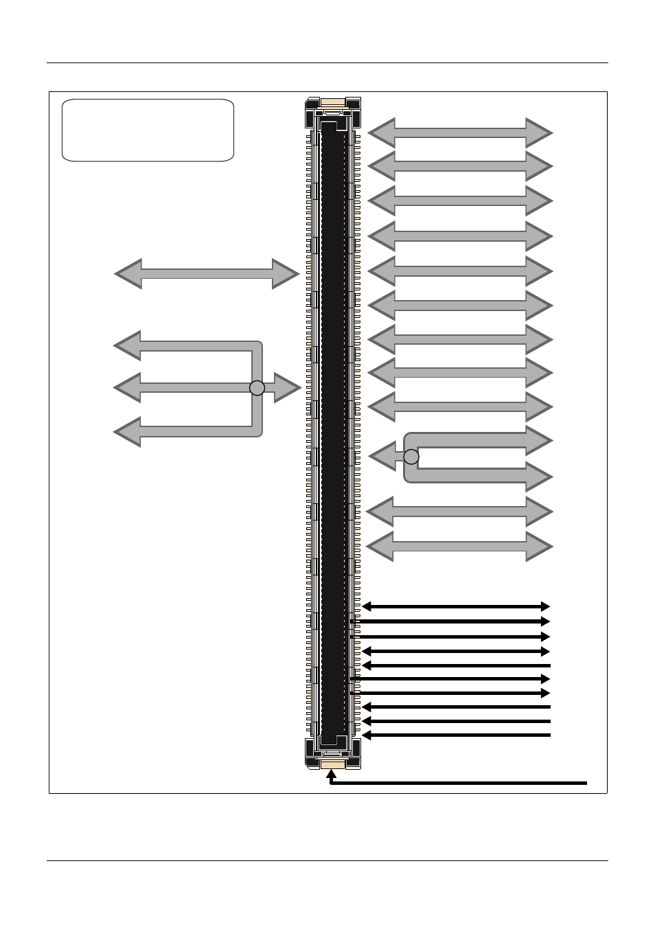
COM Express Interfaces
Figure 2:
COM Express Type 10 Connector Layout
PICMG
®
COM Express
®
Carrier Board Design Guide
Rev. 2.0 / December 6, 2013
17/218
C
o
n
n
e
c
to
r
R
o
w
s
A
&
B
P C I E x p re s s L a n e s 0 -3
E x p re s s C a r d 0 -1
L P C B u s
I²C B u s
S M B u s
A C ’9 7 S D O U T, S D IN (0 :2 ) / H D A
U S B 2 .0 P o rts 0 -7
S ATA 0-1
L A N P o rt
+ 1 2 V, V B A T, + 5 V S ta n d b y, G N D
LVDS (A, dedicated I²C)
GPI[0:3] GPO[0:3] / SDIO
W atchdog Timeout
Speaker Out
External BIOS ROM Support / SPI
System Reset
Carrier Board Reset
Suspend Control
PCI Express W ake Up Signal
General Purpose W ake Up Signal
Power Good
USB 3.0 Signals for Port 0-1
eDP (dedicated I²C )
2x serial port (1 optional CAN)
FAN Control
COM Express Module
Type 10
DisplayPort
DVI/HDMI
SDVO
DDI0
OR
OR
Note:
This diagram shows feature sets
available on these connectors.
For pin assignments and actual
positions on the connectors, refer
to the COM.0 R2.1 document.
- CP3003-SA uEFI BIOS (72 pages)
- CP3003-SA (36 pages)
- CP3002 (38 pages)
- CP3002-RC uEFI (64 pages)
- CP-RIO3-05 (42 pages)
- CP3002-RC (30 pages)
- CP342 (52 pages)
- CP930 (46 pages)
- CP932 (52 pages)
- CP346 (72 pages)
- CP384 (66 pages)
- CP383 (74 pages)
- CP382 (58 pages)
- CP381 (60 pages)
- CP372 (64 pages)
- CP371 (60 pages)
- CP-RIO3-04S (38 pages)
- CP390 (36 pages)
- CPS3410 (9 pages)
- CPS3402 (9 pages)
- CPS3105 (9 pages)
- CPS3101 (9 pages)
- CPS3003-SA (19 pages)
- PB-SIO4 (34 pages)
- PB-SIO4A (34 pages)
- PB-DOUT8 (34 pages)
- VMOD-2 (82 pages)
- VSBC-32 (110 pages)
- VM42 (62 pages)
- Bootstrap Loader (24 pages)
- VMP1 with Netbootloader (120 pages)
- VMP1 (106 pages)
- NetBootLoader (86 pages)
- VMP2 (142 pages)
- VMP3 (154 pages)
- CP-RIO6-923 (32 pages)
- CP-RIO6-923-F (32 pages)
- CP-RIO6-001 (28 pages)
- CP-RIO6-001-HD-VGA (46 pages)
- CP-RIO6-M (20 pages)
- CP-RIO6-B (28 pages)
- CP6925 (42 pages)
- CP6002 uEFI BIOS (76 pages)
- CP6002 IPMI (40 pages)
- CP6002 (42 pages)