Eight-layer stack-up, Gnd plane, Gnd plane power plane power plane – Kontron COMe Starterkit Eval T2 User Manual
Page 174
Carrier Board PCB Layout Guidelines
Figure 69 above is an example of a six layer stack-up. Layers L1, L3, L4 and L6 are used for
signal-routing. Layers L2 and L5 are power and ground planes respectively.
Microstrips on Layers 1 and 6 reference solid ground and power planes on Layers 2 and 5
respectively.
Inner Layers 3 and 4 are asymmetric striplines that are referenced to planes on Layers 2 and 5.
6.2.3.
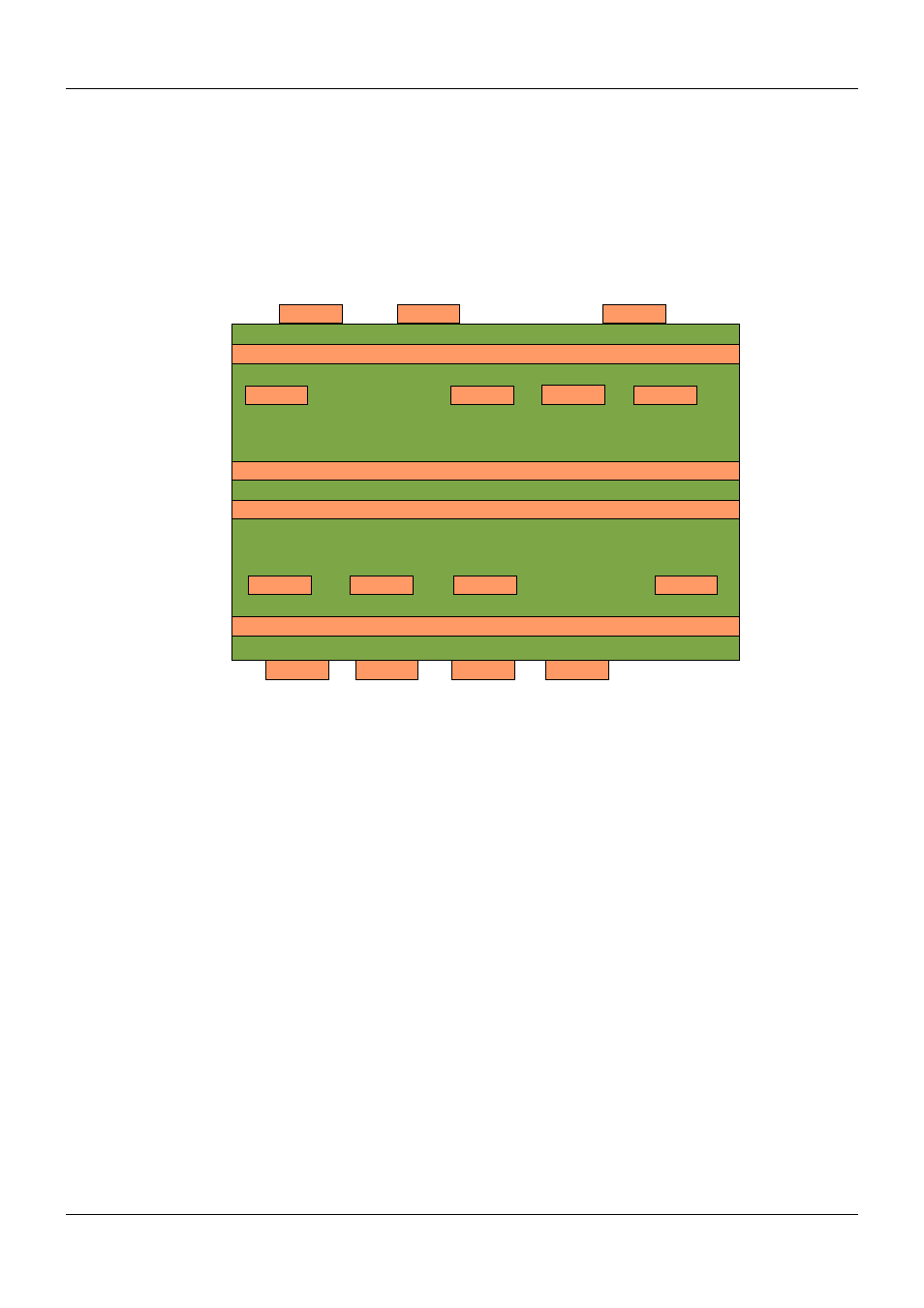
Eight-Layer Stack-up
Figure 70:
Eight-Layer Stack-up
Figure 70 above is an example of an eight layer stack-up. Layers L1, L3, L6 and L8 are used for
signal-routing. Layers L2 and L7 are solid ground planes, while L4 and L5 are used for power.
Microstrip Layers 1 and 8 reference solid ground planes on Layers 2 and 7 respectively.
Inner signal Layers 3 and 6 are asymmetric striplines that route differential signals. These
signals are referenced to Layers 2 and 7 to meet the characteristic impedance target for these
traces.
To reduce coupling to Layers 4 and 5, specify thicker prepreg to increase layer separation.
PICMG
®
COM Express
®
Carrier Board Design Guide
Rev. 2.0 / December 6, 2013
174/218
GND Plane
GND Plane
Power Plane
Power Plane
L 1
L 2
L 3
L 4
L 5
L 6
L 7
L 8