Lpc reset signal – Kontron COMe Starterkit Eval T2 User Manual
Page 112
COM Express Interfaces
Carrier designers should not buffer LPC_CLK for maximum Module interoperability. The COM
Express specification intends for a single load on the clock but experience has shown that two
devices can be driven if both devices are within 2" of each other.
2.16.2.2.
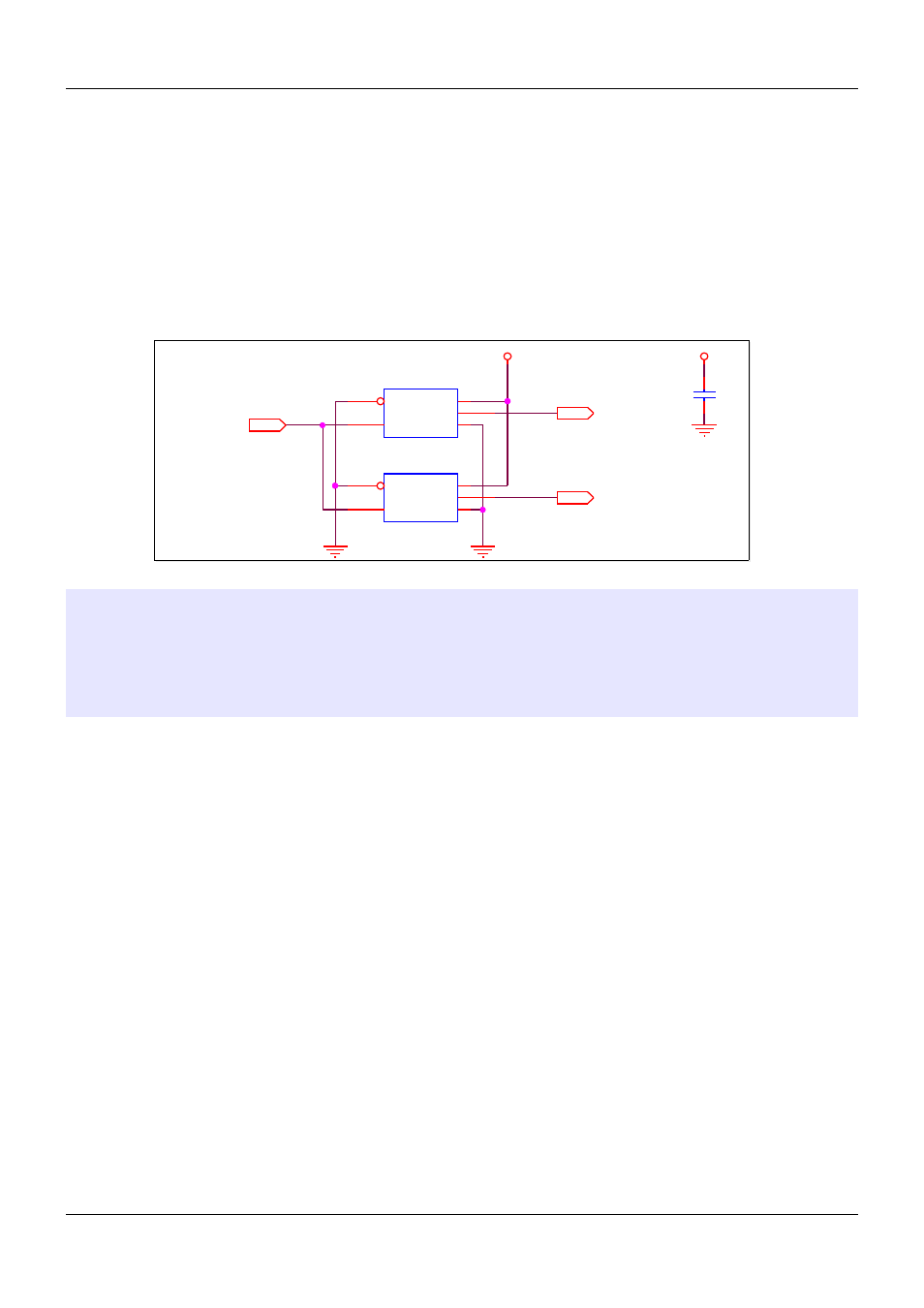
LPC Reset Signal
The LPC interface should use the signal 'CB_RESET#' as its reset input. This signal is issued by
the COM Express Module as a result of a low 'SYS_RESET#', a low 'PWR_OK' or a watchdog
timeout event. If there are multiple LPC devices implemented on the Carrier Board, it is
recommended to split the signal 'CB_RESET#' so that each LPC device will be provided with a
separate reset signal. Therefore a buffer circuit like the one shown in Figure 42 below should be
used.
Figure 42:
LPC Reset Buffer Reference Circuitry
Note:
The LPC Firmware Hub section has been moved to section 9 'Appendix A:
Deprecated Features' on page 203 below in this version of the Carrier Design
Guide. LPC Firmware hubs were typically used for Carrier based BIOS in
previous generation designs. A Carrier based BIOS is now typically support
on SPI. See section 2.17 'SPI – Serial Peripheral Interface Bus' on page 118
below for more information.
PICMG
®
COM Express
®
Carrier Board Design Guide
Rev. 2.0 / December 6, 2013
112/218
VCC_3V3
VCC_3V3
CEX
CB_RESET#
IO_RST#
FWH_RST#
C174
100n
C174
100n
U2D
74LVX125T
U2D
74LVX125T
OE#
13
IN
12
VCC
14
GND
7
OUT
11
U2C
74LVX125T
U2C
74LVX125T
OE#
10
IN
9
VCC
14
GND
7
OUT
8