Routing considerations, Com express interfaces, Picmg – Kontron COMe Starterkit Eval T2 User Manual
Page 69: Com express
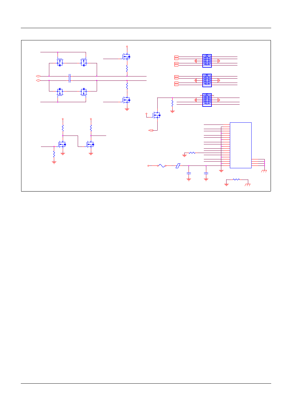
COM Express Interfaces
Figure 25:
DisplayPort implementation of MXM interface (one channel)
Following notes apply to Figure 24: MXM Reference Schematics and Figure 25: DisplayPort
implementation of MXM interface (one channel).
The reference designs supports a MXM card with two Display Port interfaces. The primary
interface between the Module and MXM Card is x16 PCI Express. The RX DC blocking
capacitors reside on the Carrier, the TX DC blocking capacitors reside on the COM Express
Module. A MXM card can support PCI Express Gen1, Gen2, or Gen3. The resistor R121 is used
to set the PCI Express voltage swing. The SMBus can be used for sideband communication with
the MXM Module. The MXM card is powered from the non-standby rail so the “S0” SMBus
signals are used. MXM_PWR_EN should be asserted no sooner than 1ms after the power to the
MXM card is stable. PEG_CLK_REQ# can be used to disable the PCI Express clock when a
MXM card is not installed to minimize emissions.
The reference schematic shows a dual mode Display Port implementation. Diodes D7, D8, and
D9 clamp ESD. T6 prevents back driving of voltage if the monitor is on and the carrier power is
off. FETs T5 and T37 level shift the cable adapter detect signal. The cable adapter detect is
used to select between HDMI and Display Port. When HDMI is selected, the AUX channel is
used as an I2C interface. The DC blocking capacitors are removed (shorted out) and pull-ups
enabled. When Display Port is selected the AUX channel is a differential pair with the DC
blocking capacitors.
2.6.3.
Routing Considerations
MXM card power requirements can be large. Note that the MXM specification allows up to 10A
of 12V, 2.5A of 5V and 1A of 3.3V. Use appropriate trace width and number of vias to deliver the
required power. The PCI Express signals should follow the routing guidelines found in chapter
2.4.4. 'Routing Considerations' on page 53 above.
PICMG
®
COM Express
®
Carrier Board Design Guide
Rev. 2.0 / December 6, 2013
69/218
DP1_CON_HPD
DP1_CON_HPD
DP1_LANE1-
DP1_LANE1+
DP1_LANE0-
DP1_LANE0+
DP1_LANE0-
DP1_LANE0+
DP1_LANE1-
DP1_LANE1+
DP1_LANE2+
DP1_LANE2-
DP1_LANE2-
DP1_LANE2+
DP1_LANE3-
DP1_LANE3+
DP1_LANE3-
DP1_LANE3+
DP1_CON_AUX-
DP1_CON_AUX+
DP1_CON_AUX-
DP1_CON_AUX+
DP1_CON_HPD
DP1_CON_AUX+
DP1_CON_AUX-
DP1_LANE0-
DP1_LANE0+
DP1_LANE1+
DP1_LANE1-
DP1_LANE2+
DP1_LANE2-
DP1_LANE3-
DP1_LANE3+
DP1_CON_AUX-
DP1_CON_AUX+
DP1_CAD
DP1_CAD
DP1_CFG2
DP1_CAD#
DP1_CAD#
DP1_CAD#
DP1_CAD_5V
DP1_CAD_5V
DP1_CAD_5V
VCC_5V0
SHLDGND
VCC_5V0
VCC_3V3
SHLDGND
VCC_3V3
VCC_5V0
DP1_LANE1-
DP1_LANE1+
DP1_LANE0-
DP1_LANE0+
DP1_LANE2+
DP1_LANE2-
DP1_LANE3-
DP1_LANE3+
DP1_AUX+
DP1_AUX-
DP1_HPD
Dual Mode support:
iif DP -> HDMI adapter connected (DPx_CAD = H)
- shorten DC blocking caps at AUX channel
- disconnect 100k PU/PD
prevents backdriving
if monitor is switched on
and system is off
F1
FNANOSMDM075F
F1
FNANOSMDM075F
R266
R5%1M0S02
R266
R5%1M0S02
R126
R5%100kS02
R126
R5%100kS02
T35A
TNTJD4001NG
T35A
TNTJD4001NG
2
1
6
R127
R1%10k0S02
R127
R1%10k0S02
T37
T2N7002A
T37
T2N7002A
1
2
3
T36A
TNTJD4001NG
T36A
TNTJD4001NG
2
1
6
R129
R5%1M0S02
R129
R5%1M0S02
FB33
FB60R0A6S03
FB33
FB60R0A6S03
R125
R5%100kS02
R125
R5%100kS02
C223
C100nS02V16X
C223
C100nS02V16X
R265
R5%0R0S06
R265
R5%0R0S06
D8
DRCLAMP0524P
D8
DRCLAMP0524P
1
2
3
4
5
6
7
8
9
10
D7
DRCLAMP0524P
D7
DRCLAMP0524P
1
2
3
4
5
6
7
8
9
10
T6
T2N7002A
T6
T2N7002A
1
2
3
C227
C100nS02V16X
C227
C100nS02V16X
T34
T2N7002A
T34
T2N7002A
1
2
3
C224
C100nS02V16X
C224
C100nS02V16X
R128
R5%1M0S02
R128
R5%1M0S02
D9
DRCLAMP0524P
D9
DRCLAMP0524P
1
2
3
4
5
6
7
8
9
10
R268
R1%10k0S02
R268
R1%10k0S02
T35B
TNTJD4001NG
T35B
TNTJD4001NG
5
4
3
X21
XBUDP_RA_SMD
X21
XBUDP_RA_SMD
LANE0+
1
GND
2
LANE0-
3
LANE1+
4
GND
5
LANE1-
6
LANE2+
7
GND
8
LANE2-
9
LANE3+
10
GND
11
LANE3-
12
Config1
13
Config2
14
AUX+
15
GND
16
AUX-
17
HPD
18
RTN_PWR
19
PWR
20
SHLD
21
SHLD
22
SHLD
23
SHLD
24
C226
C10uS05V16X
C226
C10uS05V16X
T36B
TNTJD4001NG
T36B
TNTJD4001NG
5
4
3
T5
T2N7002A
T5
T2N7002A
1
2
3
T33
T2N7002A
T33
T2N7002A
1
2
3