Spi reference schematics, Com express interfaces – Kontron COMe Starterkit Eval T2 User Manual
Page 119
COM Express Interfaces
Table 36:
Effect of the BIOS disable signals
BIOS_DIS1#
BIOS_DIS0# Chipset
SPI CS1#
Destination
Chipset
SPI CS0#
Destination
Carrier
SPI_CS#
SPI
Descriptor
BIOS Entry
Ref
Line
1
1
Module
Module
High
Module
SPI0/SPI1
0
1
0
Module
Module
High
Module
Carrier FWH 1
0
1
Module
Carrier
SPI0
Carrier
SPI0/SPI1
2
0
0
Carrier
Module
SPI1
Module
SPI0/SP1
3
2.17.2.
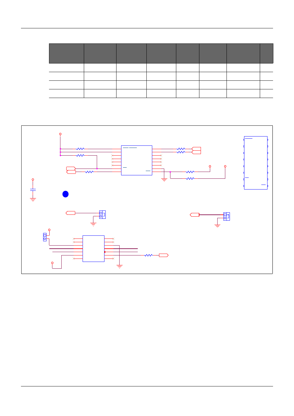
SPI Reference Schematics
Figure 46:
SPI Reference Schematics
The BIOS device shown in Figure 46: SPI Reference Schematics is an Atmel AT25DF641-S3H
flash memory device in a 16-SOIC package. The reference design above shows a socketed
implementation, using a 16-pin SOIC socket, Enplas OTS-16-1.27-04. This surface-mount
socket is footprint compatible with the SOIC-16 device, allowing for the PCB to be laid out such
that the socket or the BIOS flash device itself is soldered to the Carrier Board. Of course a
device with smaller package size (8-pin SOIC) can be used if a smaller footprint socket or device
in use.
The flash device is connected via the SPI interface to the Module. SPI_POWER, coming from
the Module is used as power source for the device.
Flash device pin 7 is the chip enable signal and is connected to the chip select pin SPI_CS# from
the Module. Pin 8 is the data output signal of the flash chip and it is connected to the Module's
SPI input SPI_MISO. PIN 15 is the data input signal of the flash chip and it is connected to the
SPI output SPI_MOSI.
PICMG
®
COM Express
®
Carrier Board Design Guide
Rev. 2.0 / December 6, 2013
119/218
i
B IO S _ D IS 0 # a nd B IO S _ D IS 1# sig n a ls h as in te rn a l p u ll-u ps o n the C O M E xp ress m o d u le
S P I_ C S #
S P I_POWER
S P I_ P O W E R
S P I_POWER
S P I_ V P P
C E X
S P I_ C S #
C E X
S P I_ C L K
C E X
S P I_ M O S I
C EX
S P I_ M IS O
C EX
B IO S _ D IS 1 #
C EX
B IO S _ D IS 0 #
JP 6
S h o rtP lu g
U 2 2
E n p la s O T S -1 6 -1 .2 7 -0 4
R S T /H O LD
V D D
N C 1
N C 2
N C 3
N C 4
C E
S O /S IO 1
S C K
16
S I/S IO 0
15
W P
9
V S S
10
N C 5
11
N C 6
12
N C 7
13
N C 8
14
J2 8
H D R _ 2 x1
R 2 0 4
R 3 8 5
0 R
5 %
DNI
R 1 7 5
C 1 91
1 0 0 n
1 0 %
5 0 V
R 1 5 3
4 k7 5 %
R 1 9 7
0 R
5 %
R 2 0 0
J2 7
H D R _ 2 x1
R212
W P
V C C
V S S
S I
S C K
C E
S O
H O L D
N C
N C
N C
N C
N C
N C
N C
N C
U 4 9
A T 2 5 D F 6 4 1 -S 3 H -T
JP 5
S h o rtP lu g
1
2
3
4
5
6
7
8
S P I_ C S #
S P I_ M IS O
S P I_ M O S I
S P I_ C L K
S P I_ P O W E R _ J
S P I_POWER
S P I_ V P P
C EX
S Y S _ R E S E T #
H D R _ 7 X 2
J3 2
I/O 1
I/O 2
V C C
C S
I/O 4
N C
G N D
C LK
M O S I
M IS O
V P P
S C L
I/O 3
S D A
R 3 5 3
0 R
5 %
J3 3
H D R _ 2 x1
DNI
4k7 5%
4k7 5%
0R 5%
0R 5%
1
3
5
7
9
11
13
2
4
6
8
10
12
14