Com express interfaces, Picmg, Com express – Kontron COMe Starterkit Eval T2 User Manual
Page 46
COM Express Interfaces
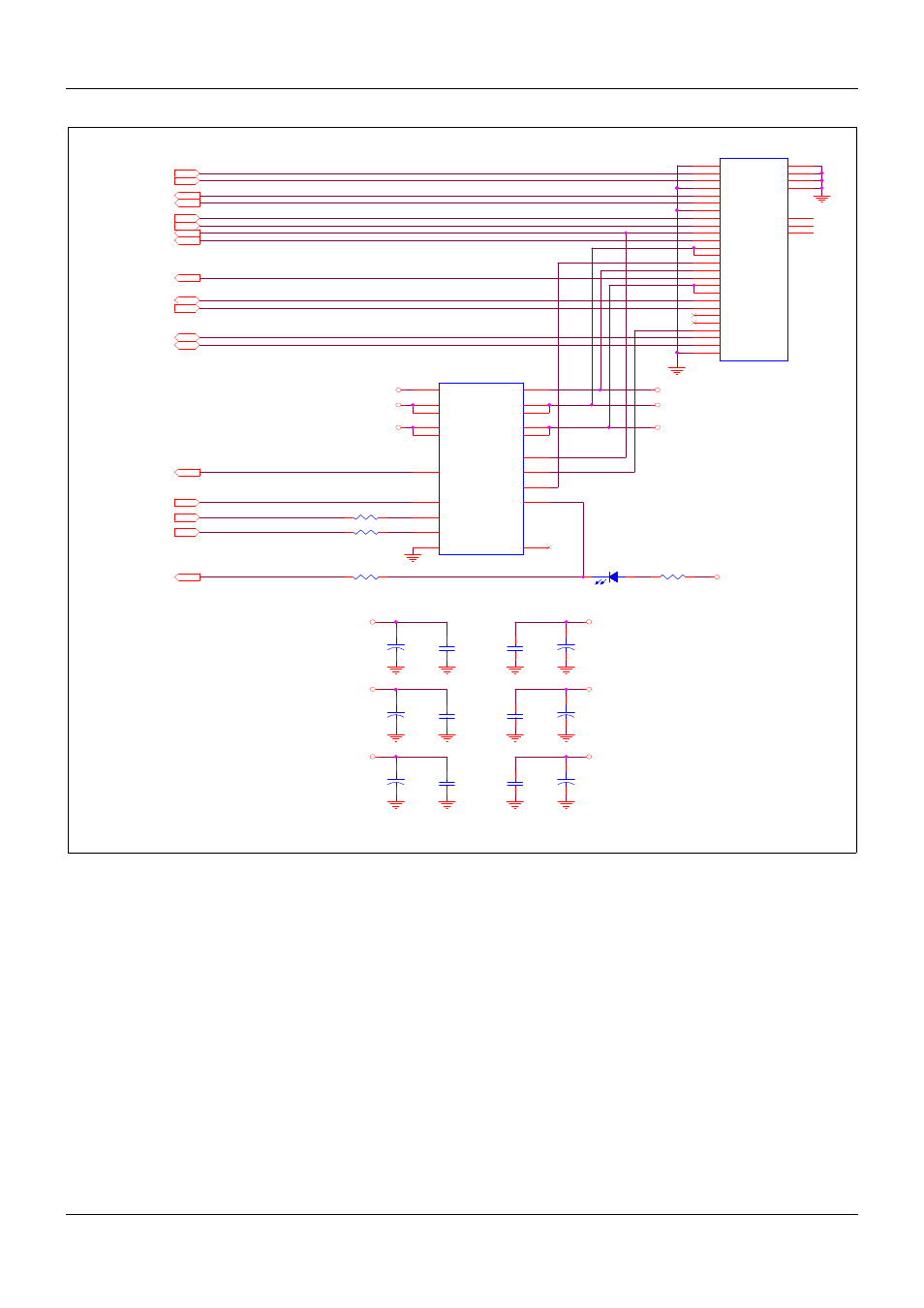
Figure 17:
PCI Express: ExpressCard Example
Figure 17 above shows an ExpressCard implementation. The example shows COM Express
PCIe lane 2 and USB port 1 used, but other assignments may be made depending on Module
capabilities and the system configuration.
Nets PCIE_TX2+ and PCIE_TX2- are sourced from the COM Express Module. These lines drive
the PCIe receivers on the Express Card. No coupling capacitors are required on the Carrier
Board. These lines are capacitively coupled on the COM Express Module.
Nets PCIE_RX2+ and PCIE_RX2- are driven by the Express Card. No coupling capacitors are
required on the Carrier Board. These lines are capacitively coupled on the Express Card.
Nets PCIE_REF_CLK1+ and PCIE_REF_CLK1- are sourced from the PCIe Reference Clock
Buffer (described earlier in Section 2.3.5.1. 'Reference Clock Buffer' on page 34 above).
CPPE# is pulled low on the Express Card to indicate that a card is present and has a PCIe
interface. CPUSB# is pulled low on the Express Card to indicate the presences of an Express
Card and a USB 2.0 interface. Either CPPE# or CPUSB# low causes the TPS2231
ExpressCard power control IC to provide power to the Express Card.
PICMG
®
COM Express
®
Carrier Board Design Guide
Rev. 2.0 / December 6, 2013
46/218
VCC_3V3_SBY
VCC_3V3_SBY
VCC_3V3
VCC_1V5
VCC_3V3_SBY
VCC_3V3
VCC_1V5
VCC_3V3_SBY_EXPCARD
VCC_3V3_EXPCARD
VCC_1V5_EXPCARD
CEX
USB1-
CEX
USB1+
CEX
SMB_DAT_S0
CEX
WAKE0#
PCIE_RX2+
CEX
PCIE_RX2-
PCIE_TX2+
CEX
PCIE_TX2-
PCIE_CLKREQ1#
PCIE_CLK_REF1-
PCIE_CLK_REF1+
CEX
SMB_CK_S0
CEX
SUS_S3#
CEX
SUS_S3#
CEX
USB_0_1_OC#
CEX
EXCD0_RST#
CEX
EXCD0_CPPE#
EXCD_PWRGOOD
Bypass caps for TPS2231
TPS2231
U3
TPS2231
NC
9
SYSRST#
1
SHDN#
2
STBY#
3
3.3IN
4
3.3IN
5
3.3OUT
6
3.3OUT
7
PERST#
8
GND
10
CPUSB#
11
CPPE#
12
1.5OUT
13
1.5OUT
14
1.5IN
15
1.5IN
16
AUXOUT
17
AUXIN
18
19
RCLKEN
OC#
20
+
C15
47 uF
1
2
R18
Do Not Stuff
C20
47 uF
J4
ExpressCard Socket
GND
1
USB_D-
2
USB_D+
3
CPUSB#
4
RSVD0
5
RSVD1
6
1.5V
9
SMB_CLK
7
SMB_DAT
8
1.5V
10
WAKE#
11
3.3VAUX
12
PERST#
13
3.3VS
14
3.3VS
15
CLKREQ#
16
CPPE#
17
REFCLK-
18
REFCLK+
19
GND
20
PERn0
21
PERp0
22
GND
23
PETn0
24
PETp0
25
GND
26
SHLD1
27
SHLD2
28
SHLD3
29
SHLD4
30
X1
X1
X2
X2
X3
X3
D1
C13
100n
C17
100n
C14
47 uF
100n
C22
R19
Do Not Stuff
R21
330R
+
C23
47 uF
1
2
C16
100n
100n
C21
C12
100n
+
C19
47 uF
1
2
R20
Do Not Stuff
C18
47 uF
VCC_3V3_SBY_EXPCARD
VCC_3V3_EXPCARD
VCC_1V5_EXPCARD
+
+
+
1
2
1
2
1
2