Reference schematics, Usb 3.0 example, Com express interfaces – Kontron COMe Starterkit Eval T2 User Manual
Page 84: Picmg, Com express
COM Express Interfaces
2.9.2.
Reference Schematics
2.9.2.1.
USB 3.0 Example
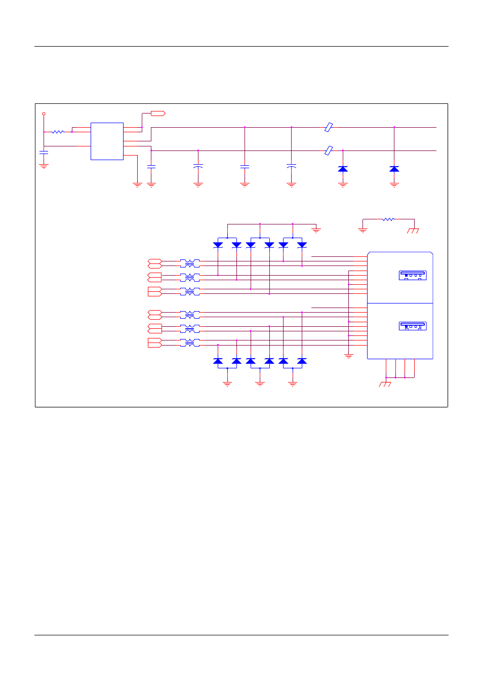
Figure 31:
USB 3.0 Example Schematic
J5 incorporates a dual USB 3.0 Type A host receptacle. Note that the SuperSpeed pins are
separate from the USB 2.0 pins.
This reference design uses an over-current detection and protection device (U10) dedicated for
USB 3.0 with 1A current limit on each USB supply voltage line.
USB_0_1_OC# is an over-current signal that is input to COM Express Module. The signal is
driven low upon detection of overload, short-circuit or thermal trip, which causes the affected
USB Port power to turn off. Do not attach pull-ups to the OC signals on the COM Express
Carrier Board; this is done on the COM Express Module.
The OC# signal is asserted until the over-current or over-temperature condition is resolved.
USB0+/- through USB1+/- from the COM Express Module are routed through a common mode
choke to reduce radiated cable emissions. The part shown is a Taiyo Yuden CM01U900T; this
device has a common mode impedance of approximately 90 Ω at 100MHz. The common-mode
choke should be placed close to the USB connector. The SuperSpeed Signals
USB_SSR/TX0+/- through USB_SSR/TX1+/- from the COM Express Module are also routed
through a common mode choke to reduce radiated cable emissions. The part shown is a Taiyo
Yuden CM01S600T; this device has a common mode impedance of approximately 60 Ω at
100MHz. The common-mode choke should be placed close to the USB connector.
PICMG
®
COM Express
®
Carrier Board Design Guide
Rev. 2.0 / December 6, 2013
84/218
1A
1A
2A
USB0_C+
V5.0_USB1_SW
V5.0_USB0_SW
V5.0_USB0_C
V5.0_USB1_C
USB_SSTX0_C-
USB_SSRX1_C-
USB_SSRX1_C+
USB_SSTX1_C-
USB_SSTX1_C+
USB_SSRX0_C-
USB_SSRX0_C+
USB_SSTX0_C+
USB1_C+
USB1_C-
USB0_C-
V5.0_USB1_C
V5.0_USB0_C
V5.0_USB
CEX
USB0+
CEX
USB0-
CEX
USB1+
CEX
USB1-
CEX
USB_0_1_OC#
CEX
USB_SSTX0-
CEX
USB_SSTX0+
CEX
USB_SSTX1+
CEX
USB_SSTX1-
C59
100n
10%
50V
FB14
CM01S600T
+
C110
220u
16V
20%
D9
ESD5V3U2U-03LRH
1
2
3
R27
0R 5%
FB18
CM01U900T 20V
FB40
60R@ 100MHz
D7
ESD5V3U2U-03LRH
1
2
3
FB39
60R@ 100MHz
C124
100n
10%
50V
2
1
J5
Foxconn UEA1112C-8HS6-4F
S1
S1
S2
S2
S3
S3
S4
S4
VBUS2
D2-
D2+
GND2
VBUS1
D1-
D1+
GND1
StdA-SSRX1-
StdA-SSRX1+
GND-DRAIN1
StdA-SSTX1-
StdA-SSTX1+
StdA-SSRX2-
StdA-SSRX2+
GND-DRAIN2
StdA-SSTX2-
StdA-SSTX2+
D27A
MMBZ6V2ALT1G
MMBZ6V2ALT1G
1
3
FB16
CM01S600T
U10
TPS206
VCC
2
EN1
3
EN2
4
GND
1
OUT1
7
OC1#
8
OC2#
5
OUT2
6
D12
ESD5V3U2U-03LRH
1
2
3
D11
ESD5V3U2U-03LRH
1
2
3
D8
ESD5V3U2U-03LRH
1
2
3
D27B
MMBZ6V2ALT1G
MMBZ6V2ALT1G
2
3
FB15
CM01S600T
C58
100n
10%
50V
FB13
CM01U900T 20V
D10
ESD5V3U2U-03LRH
1
2
3
+
C109
220u
16V
20%
FB17
CM01S600T
10
11
12
13
14
15
16
17
18
1
2
3
4
5
6
7
8
9
CEX
USB_SSRX1+
CEX
USB_SSRX1-
CEX
USB_SSRX0-
CEX
USB_SSRX0+
6
R4
0R
3
ENABLE_VBUS