Carrier board pcb layout guidelines, General, Pcb stack-ups – Kontron COMe Starterkit Eval T2 User Manual
Page 173: Four-layer stack-up, Six-layer stack-up, General 6.2. pcb stack-ups, 'carrier board pcb layout guidelines, L1 l2 l3 l4, Gnd plane power plane, Power plane gnd plane

Carrier Board PCB Layout Guidelines
6.
Carrier Board PCB Layout Guidelines
6.1.
General
6.2.
PCB Stack-ups
Note
Section 6 'Carrier Board PCB Layout Guidelines' assumes a thickness for the
carrier PCB to be 0.0625 inches. Other PCB mechanics are possible but the
described Stack-ups need to be adapted.
6.2.1.
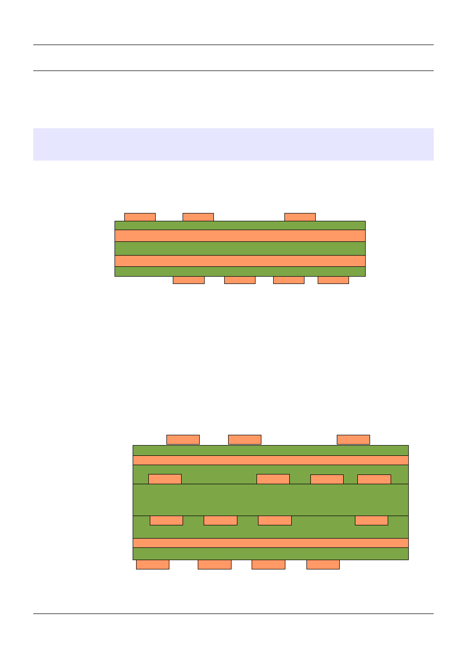
Four-Layer Stack-up
Figure 68:
Four-Layer Stack-up
Figure 68 above is an example of a four layer stack-up. Layers L1 and L4 are used for signal
routing.
Layers L2 and L3 are used for solid ground and power planes respectively.
Microstrips on Layers 1 and 4 reference ground and power planes on Layers 2 and 3
respectively.
In some cases, it may be advantageous to swap the GND and PWR planes. This allows Layer 4
to be GND referenced. Layer 4 is clear of parts and may be the preferred primary routing layer.
6.2.2.
Six-Layer Stack-up
Figure 69:
Six-Layer Stack-up
PICMG
®
COM Express
®
Carrier Board Design Guide
Rev. 2.0 / December 6, 2013
173/218
GND Plane
Power Plane
L1
L2
L3
L4
Power Plane
GND Plane
L 1
L 2
L 3
L 4
L 5
L 6
