Device-down considerations, Clock buffer, Routing considerations – Kontron COMe Starterkit Eval T2 User Manual
Page 151: General pci signals, Pci clock routing
COM Express Interfaces
2.23.2.3.
Device-Down Considerations
2.23.2.4.
Clock Buffer
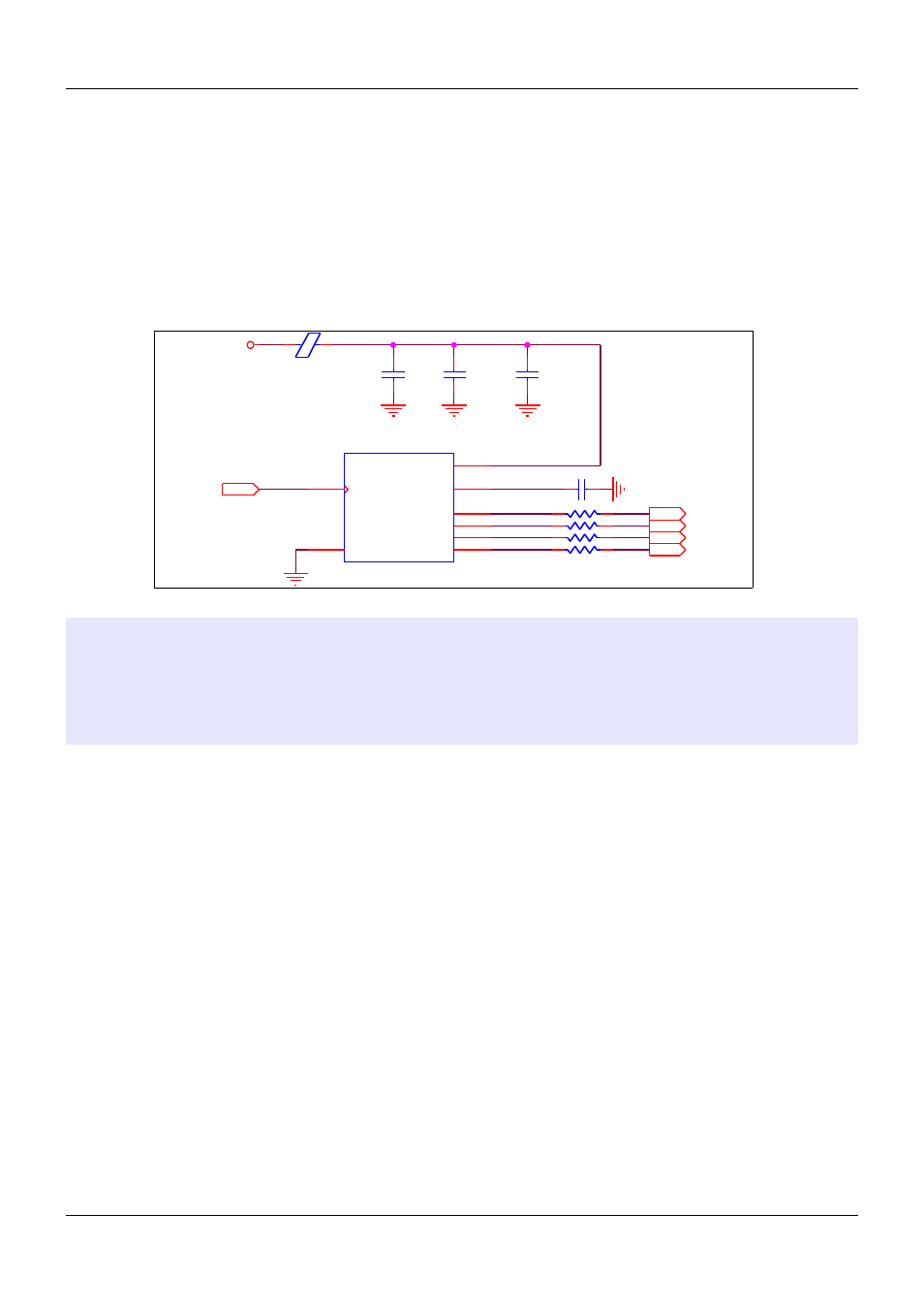
The COM Express Specification only supports a single PCI clock signal called 'PCI_CLK' to be
used on the Carrier Board. If there are multiple devices or slots implemented on the Carrier
Board, a zero delay clock buffer is required to expand the number of PCI clocks so that each
device or each bus slot will be provided with a separate clock signal. Figure 61 below shows an
example using the Texas Instruments 'CDCVF2505' zero delay clock buffer providing four output
clock signals with spread spectrum compatibility .
Figure 61:
PCI Clock Buffer Circuitry
Note:
In accordance with the 'PCI Local Bus Specification Revision 2.3', the PCI
clock signal requires a rise and fall time (slew rate) within 1V/ns and 4V/ns.
The slew rate must be met across the minimum peak-to-peak portion of the
clock wave form, which is between 0.66V and 1.98V for 3.3V clock signaling.
These parameters are very critical for EMI and must be observed during
Carrier Board layout when implementing the PCI Bus.
2.23.3.
Routing Considerations
2.23.3.1.
General PCI Signals
Route the PCI bus with 55-Ω, single-ended signals. The bus may be referenced to ground
(preferred), or to a well-bypassed power plane, or a combination of the two. Point-to-point
(daisy-chain) routing is preferred, although stubs up to 1.5 inches may be acceptable.
See Section 6.6.1. 'PCI Trace Routing Guidelines' on page 191 for a summary of trace routing
parameters and guidelines.
2.23.3.2.
PCI Clock Routing
Particular attention must be paid to the PCI clock routing. The PCI Local Bus specification
requires a maximum propagation delay for the clock signals of 10ns within a propagation skew of
2ns @ 33MHz between the several clock signals.
The COM Express Specification allows 1.6ns ± 0.1ns @ 33MHz propagation delay for the PCI
clock signal beginning from the Module pin to the destination pin of the PCI device. The
propagation delay is dependent on the trace geometries, PCB stack-up and the PCB dielectric
constant.
Calculating using a typical propagation delay value of 180ps/inch for an internal layer clock trace
of the Carrier Board, a maximum trace length of 8.88 inches is allowed.
PICMG
®
COM Express
®
Carrier Board Design Guide
Rev. 2.0 / December 6, 2013
151/218
VCC_3V3
CEX
PCI_CLK
PCI_CLK1
PCI_CLK2
PCI_CLK3
PCI_CLK4
not used
C175
C175
U20
CDCVF2505
U20
CDCVF2505
CLKIN
1
GND
4
VCC
6
CLKOUT
8
CLK1
3
CLK2
2
CLK3
5
CLK4
7
FB4 4
120R
FB4 4
120R
R13 4
22R
R13 4
22R
C174
4u7
C174
4u7
R13 5
22R
R13 5
22R
C172
10n
C172
10n
R13 6
22R
R13 6
22R
C173
100n
C173
100n
R13 3
22R
R13 3
22R