Reference schematics, Routing considerations, Com express interfaces – Kontron COMe Starterkit Eval T2 User Manual
Page 100: Picmg, Com express
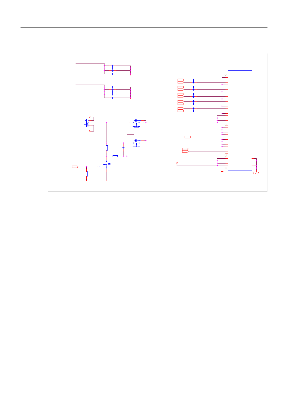
COM Express Interfaces
2.12.2.
Reference Schematics
Figure 35:
eDP Reference Schematic
The reference schematic provides a generic eDP interface. The eDP connector used in the
design is an example only. Other connectors can be used based on the design requirements.
JP83 selects 3.3 or 5V for the panel power. R1125 ensures that panel power is disabled when
the Module is powering up and before the signal is actively driven. The panel control signals
eDP_BKLT_EN, eDP_BKLT_CTRL as well as eDP_HPD are 3.3V level signals, check your
panel specifications for correct voltage levels and provide translation if necessary. The reference
design supports individual backlight control signals. It should be noted that some panels handle
these functions over the AUX channel.
2.12.3.
Routing Considerations
The traces from JP83 and associated FETs to the eDP connector carry power to the panel. The
traces should be routed with appropriate thickness to handle the current expected.
eDP_TX and eDP_AUX differential pairs should be routed as high speed differential pairs.
The panel control signals are low speed and do not require any additional care.
PICMG
®
COM Express
®
Carrier Board Design Guide
Rev. 2.0 / December 6, 2013
100/218
eDP_HPD
CEX
eDP_HPD
eDP_TX0+_C
eDP_TX0-_C
eDP_TX1+_C
eDP_TX1-_C
eDP_TX2+_C
eDP_TX2-_C
eDP_TX3+_C
eDP_TX3-_C
V12_S0_eDP_PWR
V5/V3.3_S0_eDP_PWR
eDP_BKLT_EN
eDP_BL_PWM
V12_S0_eDP_PWR
V5/V3.3_S0_eDP_PWR
GND
VCC_5V0
VCC_3V3
GND
GND
GND
GND
eDP_TX0+
eDP_TX0-
eDP_TX1+
eDP_TX1-
eDP_TX2+
eDP_TX2-
eDP_TX3+
eDP_TX3-
eDP_AUX+
eDP_AUX-
eDP_BKLT_EN
eDP_BKLT_CTRL
eDP_VDD_EN
CEX
C421
C100N03X7R
C898
C1US03V6
C885
C100N03X7R
R1123
R1%200K03
eDP
J212
JEDP_40
RSVD_1
1
H_GND_2
2
Lane3_N
3
Lane3_P
4
H_GND_5
5
Lane2_N
6
Lane2_P
7
Lane1_N
9
H_GND_8
8
Lane1_P
10
H_GND_11
11
Lane0_N
12
Lane0_P
13
H_GND_14
14
AUX_CH_P
15
AUX_CH_N
16
H_GND_17
17
LCD_VCC_18
18
LCD_VCC_19
19
LCD_VCC_20
20
LCD_VCC_21
21
LCD_Self_Test(NC)
22
LCD_GND_23
23
RSVD_40
40
BL_PWR_39
39
BL_PWR_38
38
BL_PWR_37
37
BL_PWR_36
36
RSVD_35
35
RSVD_34
34
BL_PWM_DIM(NC)
33
BL_ENABLE(NC)
32
BL_GND_31
31
BL_GND_30
30
BL_GND_29
29
BL_GND_28
28
HPD
27
LCD_GND_26
26
LCD_GND_25
25
LCD_GND_24
24
M1
41
M2
42
M3
43
M4
44
C886
C100N03X7R
C418
C100N03X7R
C887
C639
C100N03X7R
R1124
R1%10K03
C889
C100N03X7R
C419
C100N03X7R
C422
C10US06V25
C888
R1125
R1%10K03
C630
C100N03X7R
C890
C100N03X7R
C423
C100N03X7R
C420
C10US05V16
C891
Q69
BS138
C637
C100N03X7R
JP83
JMPRM254RED_LF
Q68A
QIRF7329
1
2
8
7
J104
XST1X3S
Q68B
QIRF7329
3
4
5
6
C892
C100N03X7R
CEX
CEX
VCC_12V
CEX
CEX
CEX
CEX
CEX
CEX
CEX
CEX
eDP_AUX-_C
eDP_AUX+_C
C882
C100N03X7R
CEX
CEX
C883
SHLDGND