Pci trace routing guidelines – Kontron COMe Starterkit Eval T2 User Manual
Page 191
Carrier Board PCB Layout Guidelines
6.6.1.
PCI Trace Routing Guidelines
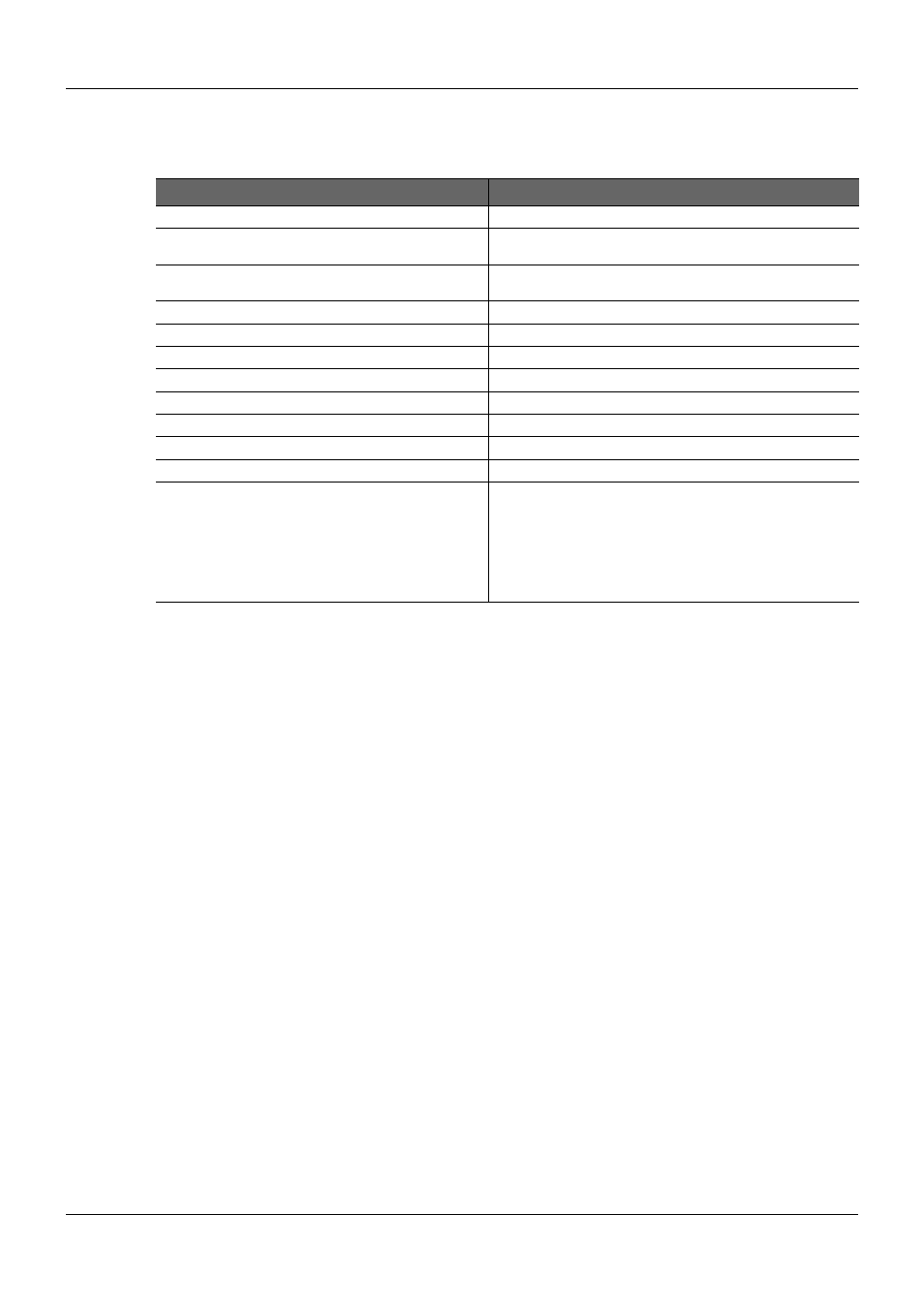
Table 69:
PCI Trace Routing Guidelines
Parameter
Trace Routing
Transfer Rate @ 33MHz
132 MB/sec
Maximum data and control signal length allowance for the
COM Express Carrier Board.
10 inches
Maximum clock signal length allowance for the COM
Express Carrier Board.
8.88 inches
Single-ended Impedance
55 Ω +/-15%
Trace width (W)
PCB stack-up dependent
Spacing between signals (inter-signal) (S)
PCB stack-up dependent
Length matching between single ended signals
Max. 200mils
Length matching between clock signals
Max. 200mils
Spacing from edge of plane
Min. 40mils
Reference plane
GND referenced preferred
Via Usage
Try to minimize number of vias
Decoupling capacitors for each PCI slot.
Min. 1x22µF, 2x 100nF @ VCC 5V
Min. 2x22µF, 4x 100nF @ VCC 3.3V
Min. 1x22µF, 2x 100nF @ +12V (if used)
Min. 1x22µF, 2x 100nF @ -12V (if used)
The decoupling capacitors for the power rails should be placed
as close as possible to the slot power pins, connected with wide
traces.
PICMG
®
COM Express
®
Carrier Board Design Guide
Rev. 2.0 / December 6, 2013
191/218