Serial ata trace routing guidelines – Kontron COMe Starterkit Eval T2 User Manual
Page 188
Carrier Board PCB Layout Guidelines
6.5.8.
Serial ATA Trace Routing Guidelines
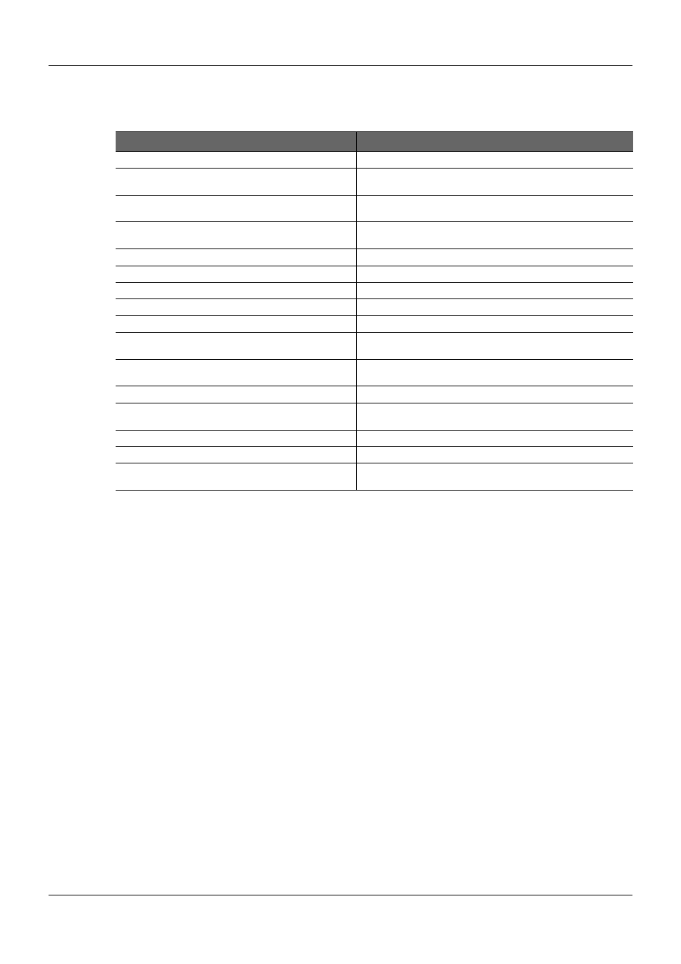
Table 67:
Serial ATA Trace Routing Guidelines
Parameter
Trace Routing
Transfer Rate
Up to 6.0 GBit/s
Maximum signal line length
(coupled traces)
5.0 inches on PCB (COM Express Module and Carrier Board. The
length of the SATA cable is specified between 0 and 40 inches)
Signal length used on COM Express Module
(including the COM Express Carrier Board connector)
2 inches
Signal length available for the COM Express Carrier
Board
3 inches, a redriver may be necessary for GEN3 signaling rates
Differential Impedance
85 Ω +/-20%
Single-ended Impedance
50 Ω +/-15%
Trace width (W)
PCB stack-up dependent
Spacing between differential pairs (intra-pair) (S)
PCB stack-up dependent
Spacing between RX and TX pairs (inter-pair) (s)
Min. 20mils
Spacing between differential pairs and high-speed
periodic signals
Min. 50mils
Spacing between differential pairs and low-speed non
periodic signals
Min. 20mils
Length matching between differential pairs (intra-pair)
Max. 5mils
Length matching between RX and TX pairs (inter-pair)
No strict length-matching requirements. Route the signals as
directly as possible.
Spacing from edge of plane
Min. 40mils
Via Usage
A maximum of 2 vias is recommended.
AC Coupling capacitors
The AC coupling capacitors for the TX and RX lines are
incorporated on the COM Express Module.
PICMG
®
COM Express
®
Carrier Board Design Guide
Rev. 2.0 / December 6, 2013
188/218