Routing considerations, General signals, Bus clock routing – Kontron COMe Starterkit Eval T2 User Manual
Page 116: Com1/com2, Figure 45: lpc serial interfaces, Com express interfaces, Picmg, Com express
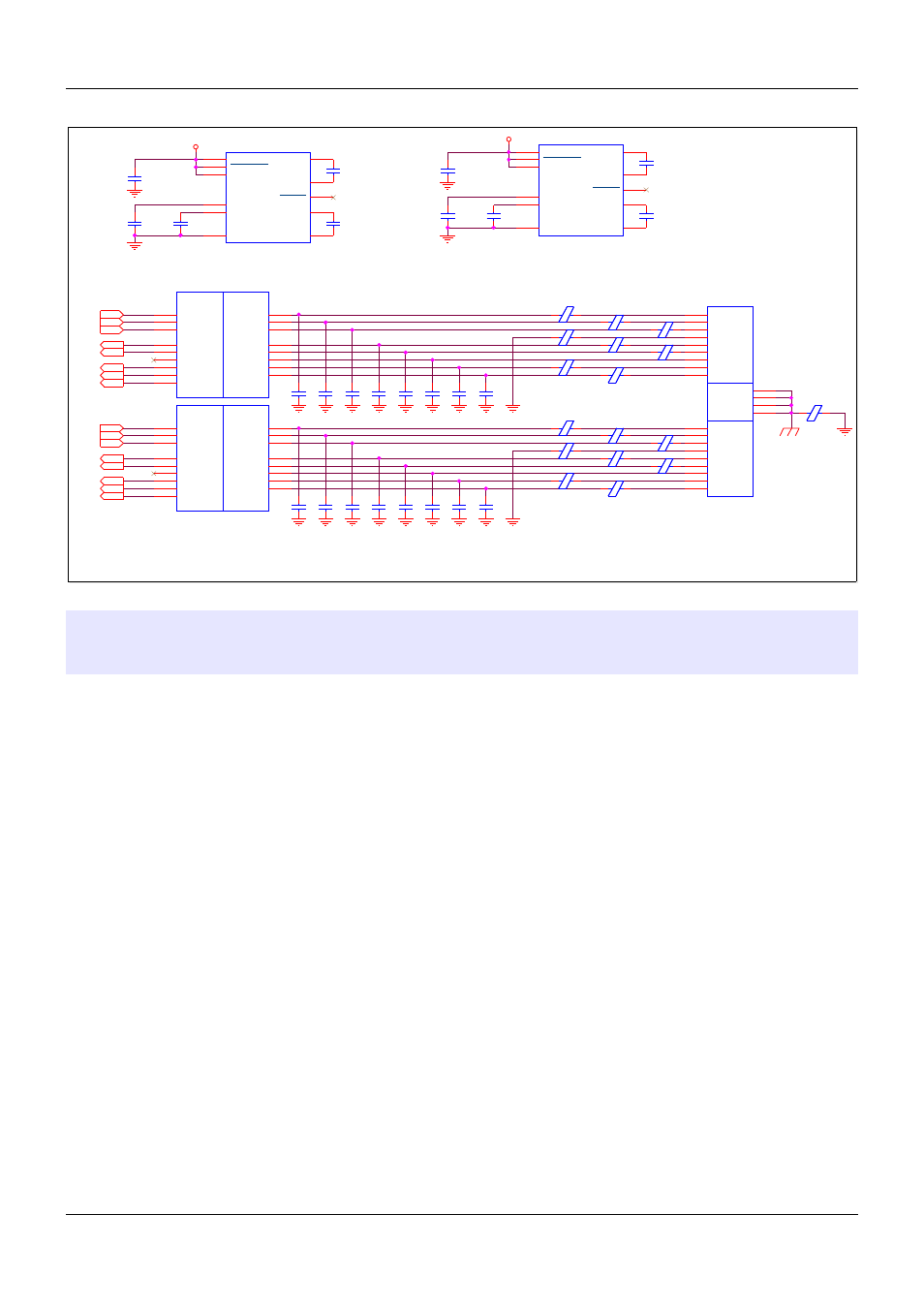
COM Express Interfaces
Figure 45:
LPC Serial Interfaces
Note:
Connection between logic GND and chassis depends on grounding
architecture. Connect GND with chassis at a single point even though this
connection is drawn on all schematic examples throughout this document.
2.16.3.
Routing Considerations
2.16.3.1.
General Signals
LPC signals are similar to PCI signals and may be treated similarly. Route the LPC bus as 55 Ω,
single-ended signals. The bus may be referenced to ground (preferred), or to a well-bypassed
power plane or a combination of the two. Point-to-point (daisy-chain) routing is preferred,
although stubs up to 1.5 inches may be acceptable. Length-matching among LPC_AD[3:0],
LPC_FRAME# are needed
See Section 6.6.3 'LPC Trace Routing Guidelines' on page 193 below.
2.16.3.2.
Bus Clock Routing
The LPC bus clock is similar to the PCI bus clock and should be treated similarly. The COM
Express Specification allows 1.6 ns +/- 0.1ns for the propagation delay of the LPC clock from the
Module pin to the LPC device destination pin. Using a typical propagation delay value of 180 ps /
inch, this works out to 8.88 inches of Carrier Board trace for a device-down application. For
device-up situations, 2.5 inches of clock trace are assumed to be on the LPC slot card (by
analogy to the PCI specification). This is deducted from the 8.88 inches, yielding 6.38 inches.
On a Carrier Board with a small form factor, serpentine clock traces may be required to meet the
clock-length requirement.
Route the LPC clock as a single-ended, 55 Ω trace with generous clearance to other traces and
to itself. A continuous ground-plane reference is recommended. Routing the clock on a single
ground referenced internal layer is preferred to reduce EMI.
PICMG
®
COM Express
®
Carrier Board Design Guide
Rev. 2.0 / December 6, 2013
116/218
VCC_5V0
VCC_5V0
TX0
TX1
RTS0#
RTS1#
DTR0#
DTR1#
RX0
RX1
CTS0#
CTS1#
DSR0#
DSR1#
DCD1#
DCD0#
RI0#
RI1#
COM1/COM2
3243E:
Maxim MAX3243E
Exar SP3243E
TI TRS3243E
FB87
600R / 0.2A
FB87
600R / 0.2A
C248
3p3
C248
3p3
FB88
600R / 0.2A
FB88
600R / 0.2A
C256
3p3
C256
3p3
FB89
600R / 0.2A
FB89
600R / 0.2A
C210
100n / 16V
C210
100n / 16V
FB91
50-Ohms@100MHz 3A
FB91
50-Ohms@100MHz 3A
FB76
600R / 0.2A
FB76
600R / 0.2A
FB90
600R / 0.2A
FB90
600R / 0.2A
U51A
3243E
U51A
3243E
VCC
26
FORCEOFF
22
FORCEON
23
V+
27
V-
3
GND
25
C1+
28
C1-
24
INVALID
21
C2+
1
C2-
2
C243
3p3
C243
3p3
S
hi
el
d
T
op
D
B
9
B
ot
to
m
D
B
9
J31
NORCOMP 189-009-613R351
S
hi
el
d
T
op
D
B
9
B
ot
to
m
D
B
9
J31
NORCOMP 189-009-613R351
RX1
A2
RI1
A9
DTR1
A4
DSR1
A6
CD1
A1
TX1
A3
GND1
A5
CTS1
A8
RTS1
A7
RX2
B2
CTS2
B8
RTS2
B7
DTR2
B4
RI2
B9
TX2
B3
GND2
B5
DSR2
B6
CD2
B1
SH1
S1
SH2
S2
SH3
S3
SH4
S4
FB78
600R / 0.2A
FB78
600R / 0.2A
C246
3p3
C246
3p3
C249
3p3
C249
3p3
C207
470n / 16V
C207
470n / 16V
C209
100n / 16V
C209
100n / 16V
FB79
600R / 0.2A
FB79
600R / 0.2A
TTL/CMOS
RS-232
U51B
3243E
TTL/CMOS
RS-232
U51B
3243E
TIN1
14
TIN2
13
TIN3
12
ROUT1
19
ROUT2
18
ROUT2B
20
ROUT3
17
ROUT4
16
ROUT5
15
TOUT1
9
TOUT2
10
TOUT3
11
RIN1
4
RIN2
5
RIN3
6
RIN4
7
RIN5
8
C250
3p3
C250
3p3
FB80
600R / 0.2A
FB80
600R / 0.2A
C216
3p3
C216
3p3
C208
470n / 16V
C208
470n / 16V
C251
3p3
C251
3p3
FB81
600R / 0.2A
FB81
600R / 0.2A
C215
100n / 16V
C215
100n / 16V
C244
3p3
C244
3p3
C252
3p3
C252
3p3
TTL/CMOS
RS-232
U52B
3243E
TTL/CMOS
RS-232
U52B
3243E
TIN1
14
TIN2
13
TIN3
12
ROUT1
19
ROUT2
18
ROUT2B
20
ROUT3
17
ROUT4
16
ROUT5
15
TOUT1
9
TOUT2
10
TOUT3
11
RIN1
4
RIN2
5
RIN3
6
RIN4
7
RIN5
8
FB82
600R / 0.2A
FB82
600R / 0.2A
C214
100n / 16V
C214
100n / 16V
C213
470n / 16V
C213
470n / 16V
FB83
600R / 0.2A
FB83
600R / 0.2A
C247
3p3
C247
3p3
C253
3p3
C253
3p3
C212
470n / 16V
C212
470n / 16V
C254
3p3
C254
3p3
FB84
600R / 0.2A
FB84
600R / 0.2A
U52A
3243E
U52A
3243E
VCC
26
FORCEOFF
22
FORCEON
23
V+
27
V-
3
GND
25
C1+
28
C1-
24
INVALID
21
C2+
1
C2-
2
FB75
600R / 0.2A
FB75
600R / 0.2A
C206
470n / 16V
C206
470n / 16V
FB85
600R / 0.2A
FB85
600R / 0.2A
C255
3p3
C255
3p3
C242
3p3
C242
3p3
FB77
600R / 0.2A
FB77
600R / 0.2A
FB86
600R / 0.2A
FB86
600R / 0.2A
C211
470n / 16V
C211
470n / 16V
C245
3p3
C245
3p3