Spi – serial peripheral interface bus, Signal definition, 17 'spi – serial peripheral interface bus – Kontron COMe Starterkit Eval T2 User Manual
Page 118: 118 below
COM Express Interfaces
2.17.
SPI – Serial Peripheral Interface Bus
The SPI interface is defined in this specification to service as an off-module option for BIOS
storage. The SPI interface replaces the LPC Firmware Hub interface, which is now considered a
legacy interface for firmware storage (LPC does continue to be used for SuperIO connectivity).
Many current chipsets only specify SPI for BIOS/Firmware storage usage, so the COM.0
specification is limited to that connectivity use-case to enable maximum compatibility across
Modules and silicon platforms. Additional features, such as SPI-based Trusted Platform Module
support might be added to a given carrier design, but compatibility is not guaranteed across
Modules.
2.17.1.
Signal Definition
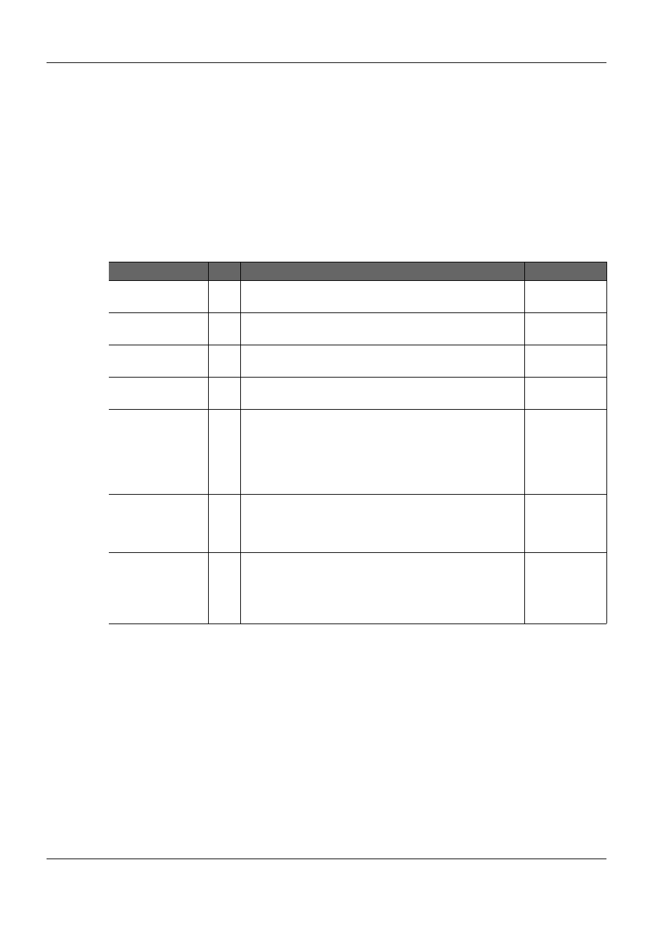
Table 35:
SPI Signal Definition
Signal
Pin
Description
I/O
SPI_CS#
B97 Chip select for Carrier Board SPI – may be sourced
from chipset SPI0 or SPI1
O CMOS –
3.3V Suspend
SPI_MISO
A92 Data in to Module from Carrier SPI
I CMOS –
3.3V Suspend
SPI_MOSI
A95 Data out from Module to Carrier SPI
O CMOS –
3.3V Suspend
SPI_CLK
A94 Clock from Module to Carrier SPI
O CMOS –
3.3V Suspend
SPI_POWER
A91 Power supply for Carrier Board SPI – sourced from
Module – nominally 3.3V. The Module shall provide a
minimum of 100mA on SPI_POWER.
Carriers shall use less than 100mA of SPI_POWER.
SPI_POWER shall only be used to power SPI devices
on the Carrier.
O – 3.3V
Suspend
BIOS_DIS0#
A34 Selection strap to determine the BIOS boot device.
The Carrier should only float these or pull them low,
please refer to for strapping options of BIOS disable
signals.
I CMOS
BIOS_DIS1#
B88 Selection strap to determine the BIOS boot device.
The Carrier should only float these or pull them low,
please refer to Table 36: Effect of the BIOS disable
signals on page 119 below for strapping options of
BIOS disable signals.
I CMOS
The signals with the “SPI_” prefix names are used to connect directly to the regarding SPI
device. SPI_CS# is the chip select signal and is usually sourced from the Module's chipset SPI0
or SPI1 signal. SPI_MISO and SPI_MOSI are the input and output signals and SPI_CLK offers
the clock from the Module to the carrier's device. The SPI_POWER pin can be used to power
the SPI devices and it should use less than 100mA in total. The signal is helpful to simplify the
SPI schematic, because the Module's SPI power domain can be either in power state S0 or in
S5.
BIOS_DIS[0:1]# signals are used to determine the boot device according to Table 36: Effect of
the BIOS disable signals below. BIOS_DIS0# (formerly known as BIOS_DISABLE# in COM.0
R1.0) is used to disable the on-module BIOS device and enable the LPC firmware hub. For SPI
BIOS flash device usage the signal BIOS_DIS1# should be activated to disable the on-module
BIOS device and enable the BIOS flash chip on the carrier.
PICMG
®
COM Express
®
Carrier Board Design Guide
Rev. 2.0 / December 6, 2013
118/218