Lan trace routing guidelines – Kontron COMe Starterkit Eval T2 User Manual
Page 187
Carrier Board PCB Layout Guidelines
6.5.7.
LAN Trace Routing Guidelines
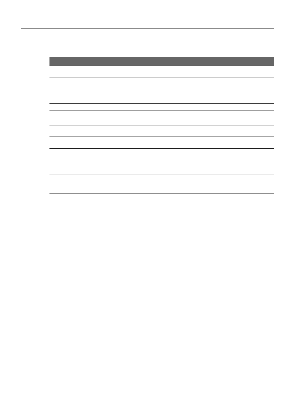
Table 66:
LAN Trace Routing Guidelines
Parameter
Trace Routing
Signal length allowance for the COM Express Carrier
Board
5.0 inches from the COM Express Module to the magnetics
Module
Maximum signal length between isolation magnetics
Module and RJ45 connector on the Carrier Board
1.0 inch
Differential Impedance
95 Ω +/-20%
Single-ended Impedance
55 Ω +/-15%
Trace width (W)
PCB stack-up dependent
Spacing between differential pairs (intra-pair) (S)
PCB stack-up dependent
Spacing between RX and TX pairs (inter-pair) (s)
Min. 50mils
Spacing between differential pairs and high-speed periodic
signals
Min. 300mils
Spacing between differential pairs and low-speed non
periodic signals
Min. 100mils
Length matching between differential pairs (intra-pair)
Max. 5mils
Length matching between RX and TX pairs (inter-pair)
Max. 30mils
Spacing between digital ground and analog ground plane
(between the magnetics Module and RJ45 connector)
Min. 60mils
Spacing from edge of plane
Min. 40mils
Via Usage
Max. of 2 vias on TX path
Max. of 2 vias on RX path
PICMG
®
COM Express
®
Carrier Board Design Guide
Rev. 2.0 / December 6, 2013
187/218