Reference schematics, General purpose serial port example, Routing considerations – Kontron COMe Starterkit Eval T2 User Manual
Page 126: C o m 1 c o m 2, No further routing considerations need to be taken, Com express interfaces, Picmg, Com express
COM Express Interfaces
2.20.2.
Reference Schematics
2.20.2.1.
General Purpose Serial Port Example
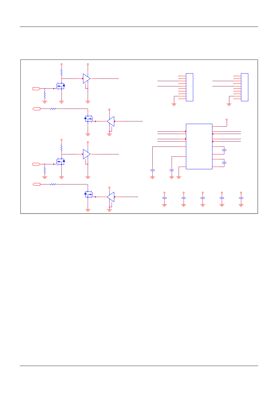
Figure 49:
General Purpose Serial Port Example
Figure 49: General Purpose Serial Port Example shows the schematic of two general purpose
serial ports with RS232 level shifter (U6). The transistor / inverter combination at the serial TX
and RX lines coming from the Module is necessary to handle the protection against VCC_12V
connection according to chapter 5.10 of COM.0 Rev. 2.1. The MAX3232CD is a dual port RS232
transceiver and handles the level shifting of the TTL signals to the regarding voltage level.
Conformance to the protection scheme defined in COM.0 Rev 2 for pins recovered from the 12V
pool results in a transfer rate limit of about 10 kbaud. If your situation requires higher speeds,
contact your Module vendor for possible work-arounds. The work-arounds likely involve
sacrificing the 12V protection as a tradeoff for higher speeds.
2.20.3.
Routing Considerations
No further routing considerations need to be taken.
PICMG
®
COM Express
®
Carrier Board Design Guide
Rev. 2.0 / December 6, 2013
126/218
C O M 1
C O M 2
S E R 0_ R X _T T L
S E R 0_ T X _ T T L
S E R 1_ T X _ T T L
S E R 1_ R X _T T L
S E R 0 _ R X _ R S 2 3 2
S E R 0 _ T X _R S 2 32
S E R 1 _ T X _R S 2 32
S E R 1 _ R X _ R S 2 3 2
S E R 0_ T X _ T T L
S E R 0 _R X _ T T L
S E R 1 _R X _ T T L
S E R 1_ T X _ T T L
S E R 0_ R X _R S 23 2
S E R 1 _ R X _ R S 2 32
S E R 1 _ T X _R S 23 2
S E R 0_ T X _ R S 23 2
VCC_3V3
VCC_3V3
VCC_3V3
VCC_3V3
VCC_3V3
VCC_3V3
C E X
S E R 0 _ R X
C E X
S E R 0 _ T X
C E X
S E R 1 _ R X
C E X
S E R 1 _ T X
C 25 7
1 0 0n
2 2 58 9
2 0 1-1 00
1 0%
5 0V
Q 9
10 2 6 2
24 1 -0 0 0
2N 7 00 2
60 V
3
1
2
C 2 40
1 0 0 n
2 2 5 8 9
2 0 1 -1 0 0
1 0 %
5 0 V
R 2 6 0
1 k
2 82 5 7
1 %
2 11 -47 9
Q 15
10 2 6 2
24 1 -0 0 0
2N 7 00 2
60 V
3
1
2
J1 0
A M P 51 0 33 0 8 -1
1 2 63 7
D T R
R T S
T X D
R X D
D C D
D S R
C T S
R I
G N D
N C
C 1 37
1 0 0 n
2 2 5 89
2 0 1 -1 0 0
1 0%
50 V
C 2 2 7
1 0 0n
2 2 58 9
2 0 1-10 0
1 0%
5 0V
Q 11
10 2 6 2
24 1 -0 0 0
2N 70 0 2
60 V
3
1
2
C 26 0
1 0 0n
2 2 58 9
2 0 1-1 00
10 %
50 V
J9
A M P 5 10 3 3 0 8-1
1 26 3 7
D T R
R T S
T X D
R X D
D C D
D S R
C T S
R I
G N D
N C
U 3 1
N C 7 S Z 0 4
1 0 4 13
0 4 3 -0 0 19 -0 0
S O T 2 3 -5
2
3
4
5
1
Q 16
10 2 6 2
24 1 -0 0 0
2N 70 0 2
6 0V
3
1
2
C 1 28
1 0 0 n
2 2 5 89
2 0 1 -1 0 0
1 0%
50 V
U 6
2 69 6 8
1 01 -31 5
M A X 3 2 32 C D
C 1 +
V +
C 1 -
C 2 +
C 2 -
V -
D O U T 2
R IN 2
V cc
G N D
D O U T 1
R IN 1
R O U T 1
D IN 1
D IN 2
R O U T 2
R 2 37
4k7
10 9 93
5 %
21 1 -0 9 4
R 2 51
4k7
10 9 93
5 %
21 1 -0 9 4
R 2 42
4 k7
1 0 9 93
5%
2 1 1 -0 94
U 2 7
N C 7 S Z 0 4
1 0 41 3
0 4 3-00 1 9 -0 0
S O T 2 3 -5
2
3
4
5
1
R 2 53
4 k7
1 0 9 93
5%
2 1 1 -0 94
C 1 3 6
1 00 n
2 25 8 9
2 01 -10 0
1 0 %
5 0 V
C 1 3 8
10 0 n
22 5 8 9
20 1 -1 0 0
1 0 %
5 0 V
R 2 4 6
1 k
2 82 5 7
1 %
2 11 -47 9
U 3 3
N C 7 S Z 0 4
1 0 41 3
0 4 3-00 1 9 -0 0
S O T 2 3 -5
2
3
4
5
1
C 12 1
1 0 0n
2 2 58 9
2 0 1-10 0
1 0%
5 0V
U 3 6
N C 7 S Z 0 4
1 0 4 13
0 4 3 -0 0 19 -0 0
S O T 2 3 -5
2
3
4
5
1
1
2
3
4
5
6
7
8
9
10
1
2
3
4
5
6
7
8
9
10
11
12
10
9
2
6
15
15
14
13
7
8
4
5
1
3
VCC_3V3
VCC_3V3
VCC_3V3
VC C_3V3
VCC_3V3
VCC _3V3