Pcie general introduction – Kontron COMe Starterkit Eval T2 User Manual
Page 30
COM Express Interfaces
2.2.
PCIe General Introduction
PCI Express provides a scalable, high-speed, serial I/O point-to-point bus connection. A PCI
Express lane consists of dual simplex channels, each implemented as a low-voltage differentially
driven transmit pair and receive pair. They are used for simultaneous transmission in each
direction. The bandwidth of a PCI Express link can be scaled by adding signal pairs to form
multiple lanes between two devices. The PCI Express specification defines x1, x2, x4, x8, x16,
and x32 link widths.
PCIe is easy to work with, but design rules must be followed. The most important design rule is
that the PCIe lanes must be routed as differential pairs. PCIe design rules are covered in detail
in Section 2.3.6 'PCI Express Routing Considerations' at page 47. Routing a PCIe link is often
easier than routing a traditional 32 bit wide PCI bus, as there are fewer lines (2 data pairs and a
clock pair for a PCIe x1 link as opposed to over 50 lines for parallel PCI). Routing a PCIe x16
graphics link is much easier than routing an AGP 8X link, as the constraints required for the PCIe
implementation are much easier than those for AGP.
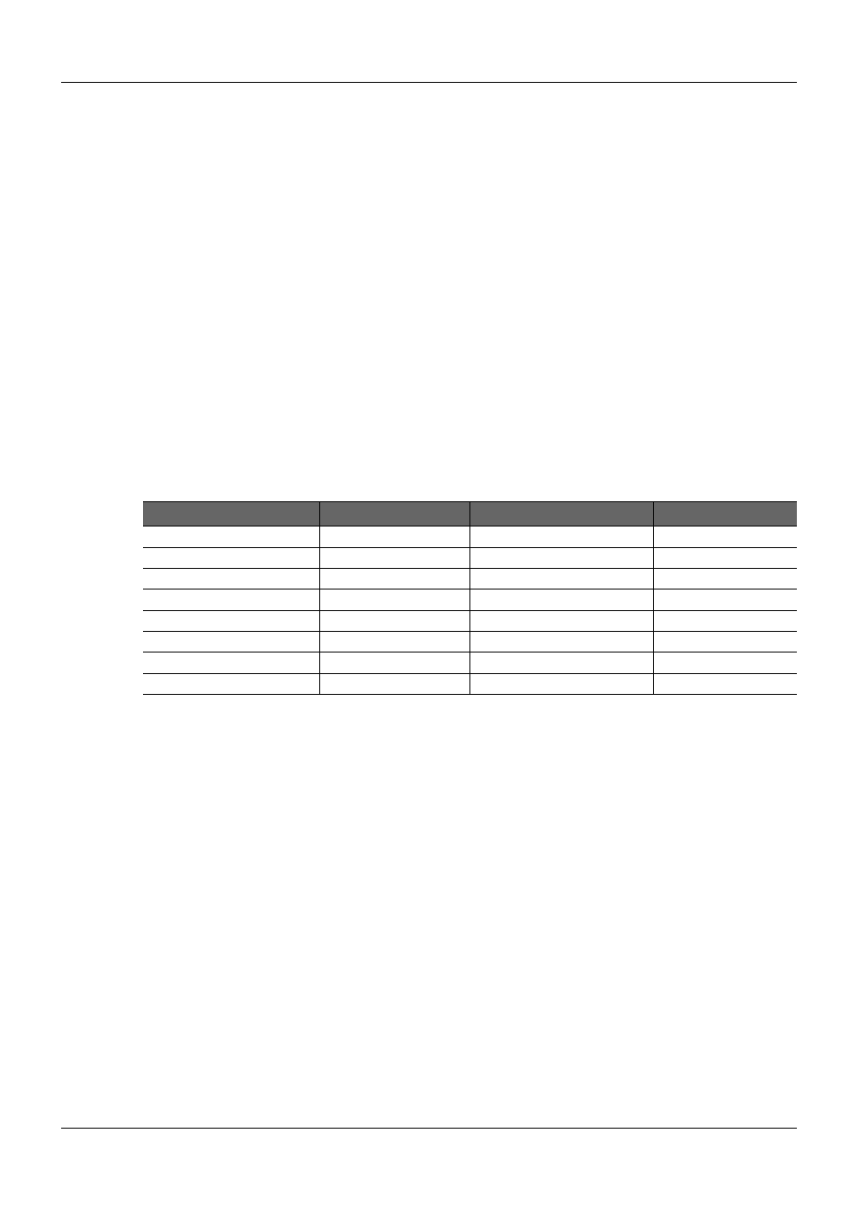
Three generations of PCI Express interfaces are available and offer different maximum transfer
rates. Each generation has slightly different routing considerations, the higher the speed the
tougher the constraints. During link training the PCI Express root complex checks which
generation can be accomplished and configures the link to the highest possible speed.
Table 5:
PCI Express Generations
Generation
PCIe 1.0/1.1
PCIe 2.0/2.1
PCIe 3.0
Symbol Rate
2.5 G Symbols/s
5.0 G Symbols/s
8.0 G Symbols/s
Line Encoding
8b10b
8b10b
128b130b
Embedded Clock
1.25 GHz
2.5 GHz
4.00 GHz
x1
250 MB/s
500 MB/s
985 MB/s
x2
500 MB/s
1000 MB/s
1969 MB/s
x4
1000 MB/s
2000 MB/s
3938 MB/s
x8
2000 MB/s
4000 MB/s
7877 MB/s
x16
4000 MB/s
8000 MB/s
15754 MB/s
The source specifications for PCI Express include the PCI Express Base Specification, the PCI
Express Card Electromechanical Specification and the PCI Express Mini Card
Electromechanical Specification.
2.2.1.
COM Express A-B Connector and C-D Connector PCIe Groups
COM Express Type 6 Modules have two groups of PCIe lanes. There is a group of up to eight
lanes; six are located on COM Express A-B connector and two on C-D connector that are
intended for general purpose use, such as interfacing the COM Express Module to Carrier Board
PCIe peripherals. A second group of PCIe lanes is defined on the COM Express C-D connector.
This group is intended primarily for the PCIe Graphics interfaces (also referred to as the PEG
interface), and is typically 16 PCIe lanes wide. For some Modules, the PEG lanes may be used
for general purpose PCIe lanes if the external graphics interface is not in use. This usage is
Module and Module chipset dependent.
COM Express Type 2 Modules also have two groups of PCIe lanes. There is a group of up to six
lanes on the COM Express A-B connector that are intended for general purpose use. A second
group of PCIe lanes is defined on the COM Express C-D connector. This group is intended
primarily for the PCIe Graphics interface and may be used for general purpose PCIe lanes if the
external graphics interface is not in use. This usage is Module and Module chipset dependent.
PICMG
®
COM Express
®
Carrier Board Design Guide
Rev. 2.0 / December 6, 2013
30/218