Pcie x1 generic device down example – Kontron COMe Starterkit Eval T2 User Manual
Page 39
COM Express Interfaces
2.3.5.5.
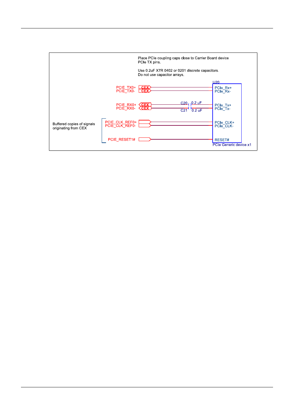
PCIe x1 Generic Device Down Example
Figure 9:
PCI Express x1 Generic Device Down Example
A generic example of a PCIe x1 device on a COM Express Carrier Board is shown in the figure
above. Only the signals that interface to the COM Express Module in the full power-on state (S0)
are shown here.
If the Carrier Board device is to support power management features, then some additional
signals may come into play. To support wake-up from Suspend states, the Carrier Board device
may assert the COM Express WAKE0# input by driving it low through an open drain device.
Some power managed Carrier Board PCIe devices may also have a CLKREQ# signal to disable
the PCIe reference clock during periods of inactivity. There is no COM Express destination for
this line. It may be used with certain clock buffers – see Figure 6 'PCIe Reference Clock Buffer'
on page 35.
Carrier Board PCIe devices may also require SMBUS support. If the Carrier Board device has a
Suspend power rail and if its SMBUS pins use that rail, then the device's SMBUS pins may be
routed directly to the corresponding COM Express SMBUS pins (SMB_CK, SMB_DAT and
SMB_ALERT#). If the Carrier Board SMBUS pins are not powered by the Suspend rail, they
must be isolated from the COM Express SMBUS lines by isolation FETs or bus switches. Refer
to Section 2.19 'System Management Bus (SMBus)' on page 123 for details.
PICMG
®
COM Express
®
Carrier Board Design Guide
Rev. 2.0 / December 6, 2013
39/218