X4 slot example, Com express interfaces, Picmg – Kontron COMe Starterkit Eval T2 User Manual
Page 38: Com express
COM Express Interfaces
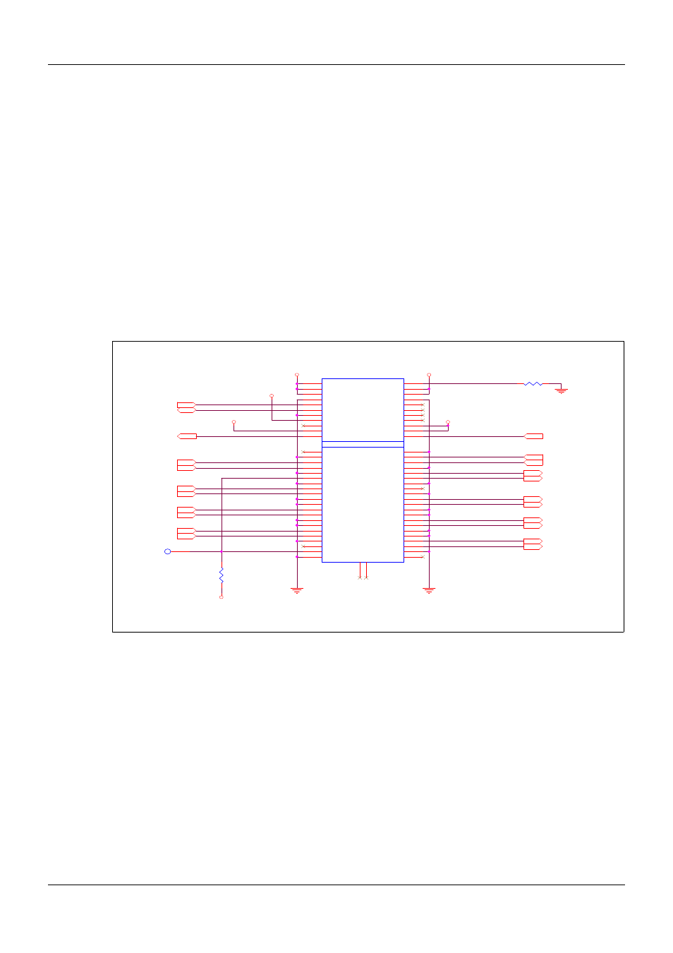
pin will be read high. Software then uses this information to apply power to the card. There is no
standard input port pin defined by COM Express for this function. For systems that are not trying
to implement hot-swap capability, it is not necessary to be able to read back the state of the
PRSNT2# pin. Hence it is shown in the figure above as being brought to a test point.
Nets SMB_CK_S0 and SMB_DAT_S0 are sourced from COM Express Module pins B13 and B14
respectively. _S0 version of SMBUS needs to be FET isolated from Module version which is on
the _S5 power rail. The SMBUS supports card-management support functions. SMBUS
software can save the state of the slot-card device before a Suspend event, report errors, accept
control parameters, return status information and card information such as a serial number.
Support for the SMBUS is optional on the slot card. Please refer to chapter 2.19 'System
Management Bus (SMBus)' on page 123 below for more information on SMBUS.
WAKE0# is asserted by the slot card to cause COM Express Module wake-up at Module pin B66.
This is an open-drain signal. It is an input to the Module and is pulled up on the Module. Other
WAKE0# sources may pull this line low; it is a shared line.
Slot JTAG pins on A5-A8 are not used.
2.3.5.4.
x4 Slot Example
Figure 8:
PCI Express x4 Slot Example
PICMG
®
COM Express
®
Carrier Board Design Guide
Rev. 2.0 / December 6, 2013
38/218
VCC_12V
VCC_12V
VCC_3V3
VCC_3V3_SBY
VCC_3V3
VCC_3V3
CEX
PCIE_TX0+
CEX
PCIE_RX0+
CEX
PCIE_TX0-
CEX
PCIE_TX1+
CEX
PCIE_TX1-
CEX
PCIE_TX2-
CEX
PCIE_TX2+
CEX
PCIE_TX3-
CEX
PCIE_TX3+
CEX
PCIE_RX0-
CEX
PCIE_RX1-
CEX
PCIE_RX1+
CEX
PCIE_RX2-
CEX
PCIE_RX2+
CEX
PCIE_RX3+
CEX
PCIE_RX3-
SMB_CK_S0
SMB_DAT_S0
CEX
WAKE0#
PCIE_RESET1#
PCIE_CLK_REF0+
PCIE_CLK_REF0-
0R
R16
R17
4.7k
TP2
Do Not Stuff
J2
J2
PCIe x4 Slot
+12V
B1
+12V
B2
+12V
B3
GND
B4
SMCLK
B5
SMDAT
B6
GND
B7
+3.3V
B8
JTAG1
B9
3.3VAUX
B10
WAKE#
B11
PRSNT1#
A1
+12V
A2
+12V
A3
GND
A4
JTAG2
A5
JTAG3
A6
JTAG4
A7
JTAG5
A8
+3.3V
A9
+3.3V
A10
PERST#
A11
RSVD
B12
GND
B13
PETp0
B14
PETn0
B15
GND
B16
PRSNT2#
B17
GND
B18
PETp1
B19
PETn1
B20
GND
B21
GND
B22
PETp2
B23
PETn2
B24
GND
B25
GND
B26
PETp3
B27
PETn3
B28
GND
B29
RSVD
B30
PRSNT2#
B31
GND
B32
GND
A12
REFCLK+
A13
REFCLK-
A14
GND
A15
PERp0
A16
PERn0
A17
GND
A18
RSVD
A19
GND
A20
PERp1
A21
PERn1
A22
GND
A23
GND
A24
PERp2
A25
PERn2
A26
GND
A27
GND
A28
PERp3
A29
PERn3
A30
GND
A31
RSVD
A32
X
1
X
1
X
2
X
2