Lvds trace routing guidelines – Kontron COMe Starterkit Eval T2 User Manual
Page 189
Carrier Board PCB Layout Guidelines
6.5.9.
LVDS Trace Routing Guidelines
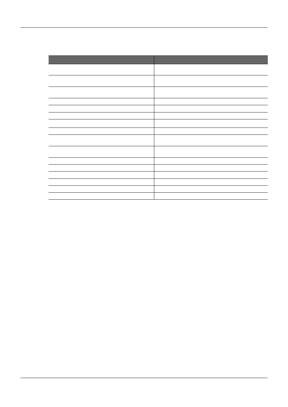
Table 68:
LVDS Trace Routing Guidelines
Parameter
Trace Routing
Maximum signal line length to the LVDS connector
(coupled traces)
8.75 inches
Signal length used on COM Express Module
(including the COM Express Carrier Board connector)
2.0 inches
Signal length to the LVDS connector available for the COM
Express Carrier Board
6.75 inches
Differential Impedance
100 Ω +/-20%
Single-ended Impedance
55 Ω +/-15%
Trace width (W)
PCB stack-up dependent
Spacing between differential pair signals (intra-pair) (S)
PCB stack-up dependent
Spacing between pair to pairs (inter-pair) (s)
Min. 20mils
Spacing between differential pairs and high-speed periodic
signals
Min. 20mils
Spacing between differential pairs and low-speed non
periodic signals
Min. 20mils
Length matching between differential pairs (intra-pair)
+/- 20mils
Length matching between clock and data pairs (inter-pair)
+/- 20mils
Length matching between data pairs (inter-pair)
+/- 40mils
Spacing from edge of plane
+/- 40mils
Reference plane
GND referenced preferred
Via Usage
Max. of 2 vias per line
PICMG
®
COM Express
®
Carrier Board Design Guide
Rev. 2.0 / December 6, 2013
189/218