Sdvo trace routing guidelines – Kontron COMe Starterkit Eval T2 User Manual
Page 185
Carrier Board PCB Layout Guidelines
6.5.5.
SDVO Trace Routing Guidelines
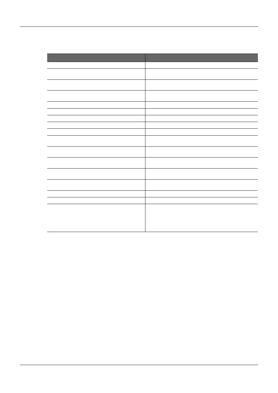
Table 64:
SDVO Trace Routing Guidelines
Parameter
Trace Routing
Transfer Rate / SDVO Lane
Up to 2.0 GBit/s
Maximum signal line length
(coupled traces)
7 inches
Signal length used on COM Express Module
(including the Carrier Board connector)
2 inches
Signal length allowance for the COM Express Carrier
Board
5 inches to SDVO device
Differential Impedance
100 Ω +/-20%
Single-ended Impedance
55 Ω +/-15%
Trace width (W)
PCB stack-up dependent
Spacing between differential pairs (intra-pair) (S)
PCB stack-up dependent
Spacing between pairs-to-pair
Min. 20mils
Spacing between differential pairs and high-speed
periodic signals
Min. 50mils
Spacing between differential pairs and low-speed non
periodic signals
Min. 20mils
Length matching between differential pairs
(intra-pair)
Max. 5mils
Length matching between differential pairs
(inter-pair)
Keep difference within a 2.0 inch delta.
Length matching between differential signal pair and
differential clock pair
Max. 5mils
Spacing from edge of plane
Min. 40mils
Via Usage
Max. 4 vias per differential signal trace
AC coupling capacitors
AC coupling capacitors on the signals 'SDVO_INT+' and
'SDVOINT-' have to be implemented on the customer COM
Express Carrier Board, if the device is directly located on the
Carrier Board. When using a slot at the Carrier Board the
capacitors are located at the addon card.
Capacitor type: X7R, 100nF +/-10%, 16V, shape 0402.
PICMG
®
COM Express
®
Carrier Board Design Guide
Rev. 2.0 / December 6, 2013
185/218