Figure 3, Below – Kontron COMe Starterkit Eval T2 User Manual
Page 18
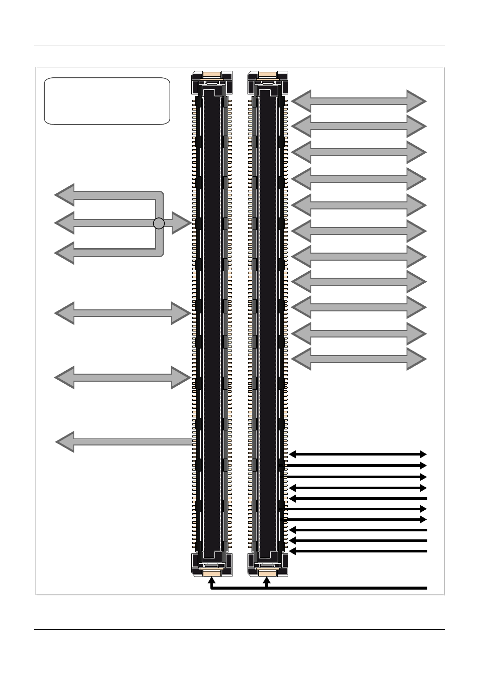
COM Express Interfaces
Figure 3:
COM Express Type 2 Connector Layout
PICMG
®
COM Express
®
Carrier Board Design Guide
Rev. 2.0 / December 6, 2013
18/218
PATA ATA 1 0 0 (1 P o rt o n ly )
P C I B u s 3 2 b it 3 3 /6 6 M H z
M o d u le Ty p e In d ic a tio n Ty p e [0 :2 ]
C
o
n
n
e
c
to
r
R
o
w
s
C
&
D
C
o
n
n
e
c
to
r
R
o
w
s
A
&
B
P C I E x p r e s s L a n e s 0 -5
E x p re s s C a rd 0 -1
L P C B u s
I²C B u s
S M B u s
A C ’9 7 S D O U T, S D IN (0 :2 ) / H D A
U S B 2 .0 P o rts 0 -7
S ATA 0-3
L A N P o rt
+ 1 2 V, V B AT, + 5 V S ta n d b y, G N D
C O M E x p re s s M o d u le
Ty p e 2
LVDS (A&B, dedicated I²C)
GPI[0:3] GPO[0:3]
W atchdog Timeout
Speaker Out
External BIOS ROM Support / SPI
System Reset
Carrier Board Reset
Suspend Control
PCI Express W ake Up Signal
General Purpose W ake Up Signal
Power Good
P C I E x p re s s G ra p h ic s x 1 6
PCI Express Lanes 16-31
OR
SDVO (dedicated I²C)
x16
VGA (dedicated DDC)
Note:
This diagram shows feature sets
available on these connectors.
For pin assignments and actual
positions on the connectors, refer
to the COM.0 R2.1 document.