Pci bus, Signal definitions – Kontron COMe Starterkit Eval T2 User Manual
Page 147
COM Express Interfaces
2.23.
PCI Bus
2.23.1.
Signal Definitions
Type 2 and 3 COM Express Modules provide a 32-bit PCI bus that can operate up to 33 MHz.
The corresponding signals can be found on the Module connector rows C and D.
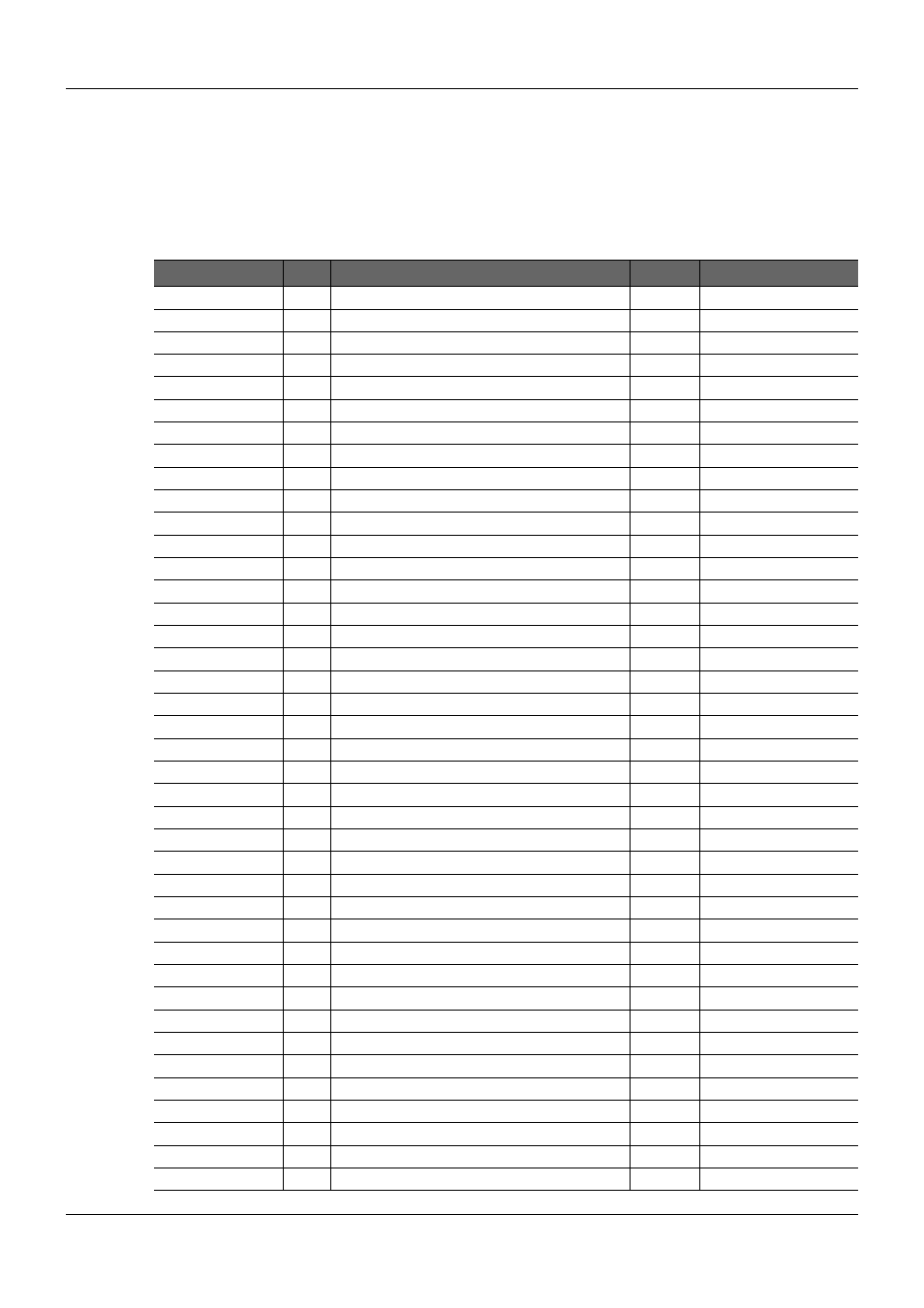
Table 48:
PCI Bus Signal Definition
Signal
Pin# Description
I/O
Comment
PCI_AD0
C24
PCI bus multiplexed address and data lines
I/O 3.3V
PCI_AD1
D22
PCI bus multiplexed address and data lines
I/O 3.3V
PCI_AD2
C25
PCI bus multiplexed address and data lines
I/O 3.3V
PCI_AD3
D23
PCI bus multiplexed address and data lines
I/O 3.3V
PCI_AD4
C26
PCI bus multiplexed address and data lines
I/O 3.3V
PCI_AD5
D24
PCI bus multiplexed address and data lines
I/O 3.3V
PCI_AD6
C27
PCI bus multiplexed address and data lines
I/O 3.3V
PCI_AD7
D25
PCI bus multiplexed address and data lines
I/O 3.3V
PCI_AD8
C28
PCI bus multiplexed address and data lines
I/O 3.3V
PCI_AD9
D27
PCI bus multiplexed address and data lines
I/O 3.3V
PCI_AD10
C29
PCI bus multiplexed address and data lines
I/O 3.3V
PCI_AD11
D28
PCI bus multiplexed address and data lines
I/O 3.3V
PCI_AD12
C30
PCI bus multiplexed address and data lines
I/O 3.3V
PCI_AD13
D29
PCI bus multiplexed address and data lines
I/O 3.3V
PCI_AD14
C32
PCI bus multiplexed address and data lines
I/O 3.3V
PCI_AD15
D30
PCI bus multiplexed address and data lines
I/O 3.3V
PCI_AD16
D37
PCI bus multiplexed address and data lines
I/O 3.3V
PCI_AD17
C39
PCI bus multiplexed address and data lines
I/O 3.3V
PCI_AD18
D38
PCI bus multiplexed address and data lines
I/O 3.3V
PCI_AD19
C40
PCI bus multiplexed address and data lines
I/O 3.3V
PCI_AD20
D39
PCI bus multiplexed address and data lines
I/O 3.3V
IDSEL for slot 0
PCI_AD21
C42
PCI bus multiplexed address and data lines
I/O 3.3V
IDSEL for slot 1
PCI_AD22
D40
PCI bus multiplexed address and data lines
I/O 3.3V
IDSEL for slot 2
PCI_AD23
C43
PCI bus multiplexed address and data lines
I/O 3.3V
IDSEL for slot 3
PCI_AD24
D42
PCI bus multiplexed address and data lines
I/O 3.3V
PCI_AD25
C45
PCI bus multiplexed address and data lines
I/O 3.3V
PCI_AD26
D42
PCI bus multiplexed address and data lines
I/O 3.3V
PCI_AD27
C46
PCI bus multiplexed address and data lines
I/O 3.3V
PCI_AD28
D44
PCI bus multiplexed address and data lines
I/O 3.3V
PCI_AD29
C47
PCI bus multiplexed address and data lines
I/O 3.3V
PCI_AD30
D45
PCI bus multiplexed address and data lines
I/O 3.3V
PCI_AD31
C48
PCI bus multiplexed address and data lines
I/O 3.3V
PCI_C/BE0#
D26
PCI bus byte enable line 0, active low
I/O 3.3V
PCI_C/BE1#
C33
PCI bus byte enable line 0, active low
I/O 3.3V
PCI_C/BE2#
C38
PCI bus byte enable line 0, active low
I/O 3.3V
PCI_C/BE3#
C44
PCI bus byte enable line 0, active low
I/O 3.3V
PCI_DEVSEL#
C36
PCI bus Device Select, active low
I/O 3.3V
PCI_Frame#
D36
PCI bus Frame control line, active low
I/O 3.3V
PCI_IRDY#
C37
PCI bus Initiator Ready control line, active low
I/O 3.3V
PCI_TRDY#
D35
PCI bus Target Ready control line, active low
I/O 3.3V
PICMG
®
COM Express
®
Carrier Board Design Guide
Rev. 2.0 / December 6, 2013
147/218