Pci express trace routing guidelines, 'pci express trace routing guidelines, 1 'pci express trace routing guidelines – Kontron COMe Starterkit Eval T2 User Manual
Page 182: Below
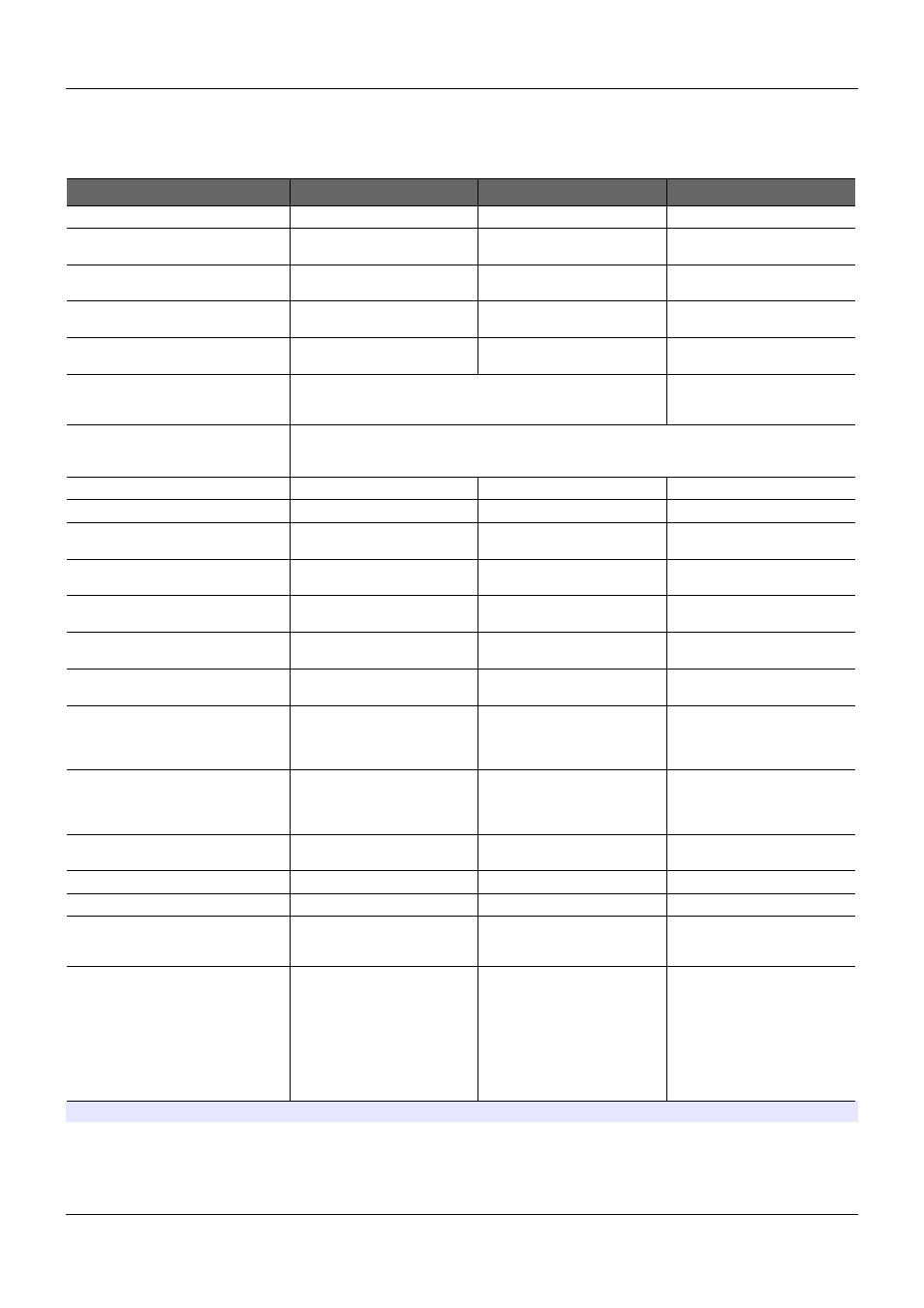
Carrier Board PCB Layout Guidelines
6.5.1.
PCI Express Trace Routing Guidelines
Table 61:
PCI Express Trace Routing Guidelines
Parameter
PCIe Gen1
PCIe Gen2
PCIe Gen3
Symbol Rate / PCIe Lane
2.5 G Symbols/s
5.0 G Symbols/s
8.0 G Symbols/s
Maximum signal line length
(coupled traces) TX and RX
21.0 inches
21.0 inches
14.0 inches
Signal length allowance on the COM
Express Carrier Board to PCIe device
15.85 inches
15.85 inches
10.0 inches
Signal length allowance on the COM
Express Carrier Board to PCIe slot
9.00 inches
9.00 inches
4.0 inches
PCI-SIG: Differential impedance
recommendation
100 Ω +/-20%
85 Ω +/-15%
85 Ω +/-15%
COMCDG Rev. 1.0: Differential
impedance recommendation for a
GEN1 and GEN2 design
92 Ω +/-10%
-
COMCDG Rev. 2.0: Differential
impedance recommendation for
new Carrier designs
85 Ω +/-15%
Single-ended Impedance
55 Ω +/-15%
50 Ω +/-15%
50 Ω +/-15%
Trace width (W)
PCB stack-up dependent
PCB stack-up dependent
PCB stack-up dependent
Spacing between differential pairs
(intra-pair) (S)
PCB stack-up dependent
PCB stack-up dependent
PCB stack-up dependent
Spacing between RX and TX pairs
(inter-pair) (s)
Min. 20mils
Min. 20mils
Min. 20mils
Spacing between differential pairs and
high-speed periodic signals
Min. 50mils
Min. 50mils
Min. 50mils
Spacing between differential pairs and
low-speed non periodic signals
Min. 20mils
Min. 20mils
Min. 20mils
Length matching between differential
pairs (intra-pair)
Max. 5mils
Max. 5mils
Max. 5mils
Length matching between RX and TX
pairs (inter-pair)
No strict electrical requirements.
Keep difference within a 3.0
inch delta to minimize latency.
No strict electrical requirements.
Keep difference within a 3.0 inch
delta to minimize latency.
No strict electrical requirements.
Keep difference within a 3.0
inch delta to minimize latency.
Length matching between reference
clock differential pairs REFCLK+ and
REFCLK-
(intra-pair)
Max. 5mils
Max. 5mils
Max. 5mils
Length matching between reference
clock pairs (inter-pair)
No electrical requirements.
No electrical requirements.
No electrical requirements.
Reference plane
GND referenced preferred
GND referenced preferred
GND referenced preferred
Spacing from edge of plane
Min. 40mils
Min. 40mils
Min. 40mils
Via Usage
Max. 2 vias per TX trace
Max. 4 vias per RX trace
Max. 2 vias per TX trace
Max. 4 vias per RX trace
Max. 2 vias / TX
Max. 4 vias / RX (to device)
Max. 2 vias / RX (to slot)
AC coupling capacitors
The AC coupling capacitors for
the TX lines are incorporated on
the COM Express Module.
The AC coupling capacitors for
RX signal lines have to be
implemented on the customer
COM Express Carrier Board.
Capacitor type: X7R, 100nF +/-
10%, 16V, shape 0402.
The AC coupling capacitors for
the TX lines are incorporated on
the COM Express Module.
The AC coupling capacitors for
RX signal lines have to be
implemented on the customer
COM Express Carrier Board.
Capacitor type: X7R, 100nF +/-
10%, 16V, shape 0402.
The AC coupling capacitors for
the TX lines are incorporated on
the COM Express Module.
The AC coupling capacitors for
RX signal lines have to be
implemented on the customer
COM Express Carrier Board.
Capacitor type: X7R, 200nF +/-
10%, 16V, shape 0402.
PICMG
®
COM Express
®
Carrier Board Design Guide
Rev. 2.0 / December 6, 2013
182/218