Hapter, Configuring the current minor loop, Block. see figure 6.2. the input to the – Rockwell Automation FlexPak 3000 Digital DC Drive Version 4.3 User Manual
Page 71: Regulator block diagram
Configuring the Current Minor Loop
6-1
C
HAPTER
6
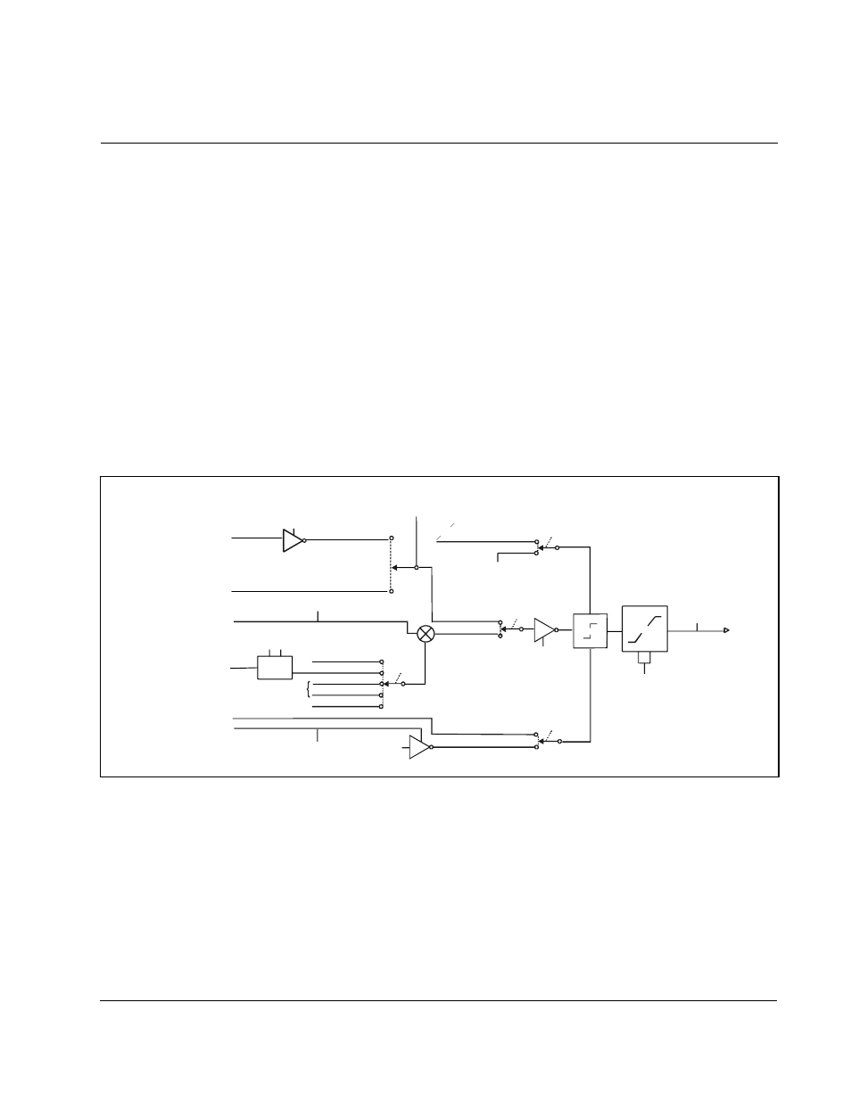
Configuring the Current Minor Loop
In all FlexPak 3000 drive configurations, the central control loop is the current minor
loop (
CML
). This is the control loop that regulates the amount of current flowing
through the motor armature.
The
CML
is a simple control loop composed of a reference path, a feedback path, and
a forward path that includes a proportional and integral (
PI
) block. See figure 6.2. The
input to the
PI
block, known as the error, is the difference between the reference and
feedback. The output of the
PI
block determines the level of current flowing through the
motor armature. When a reference change occurs, the error becomes non-zero,
causing the
PI
block output to change. This results in a higher or lower level of current
flowing through the armature until the feedback again becomes equal to the reference.
Figure 6.1 shows the details of the
CML
reference path. Figure 6.2 shows the details of
the
CML
regulator block diagram.
Figure 6.1 – Current Minor Loop Reference Path Block Diagram
(SPD LOOP OUTPUT)
POSITIVE
CURRENT LIM
CML REF
LIMIT SELECT
*SPD LOOP CUR LIM
REGISTER
*SPEED/VOLTAGE
+
+
CURRENT/TORQUE
(J15 REGULATOR
TYPE)
HI
LO
LIMIT
EN
UNDERWIND
ENABLE
From Network
0
MAXIMUM
CURRENT
Software
Scaling
NORMALIZED
INERTIA
NETW IN REG 1, 2, 3
*NONE
INTERNAL
ANALOG IN 1
ANALOG IN 2
INERTIA
COMP
SELECT
CML REF
RATE LIMIT
RATELIM
ACC
DEC
(CML
REFERENCE)
* = Default Selection
EN
NEGATIVE
CURRENT LIM
CML REF
LIMIT SELECT
*SPD LOOP PI LIMITS
REGISTER
NEG CUR LIM
INV EN
ENABLED
*DISABLED
EN
F W D / R E V
OCL TYPE3
POSN REG EN
From Figure 4.2,
Speed
Reference Source Select
Block Diagram
From Figure 5.1,
Speed Loop Block
S-curve rate output from
Figure 4.5,
Speed Reference
Ramp Block Diagram
To
Figure 6.2,
Current
Minor Loop
Block
Diagram
From Figure 5.1,
Speed
Loop Block Diagram
From Figure 9.1,
Outer
Control Loop Block
Diagram
From Figure 5.1,
Speed Loop Block Diagram
From Figure 11.2,
Analog Inputs Block
Diagram