3 configuring the analog outputs, P.420), Anlg – Rockwell Automation FlexPak 3000 Digital DC Drive Version 4.3 User Manual
Page 124: Gain
11-8
FlexPak 3000 DC Drive Software Reference
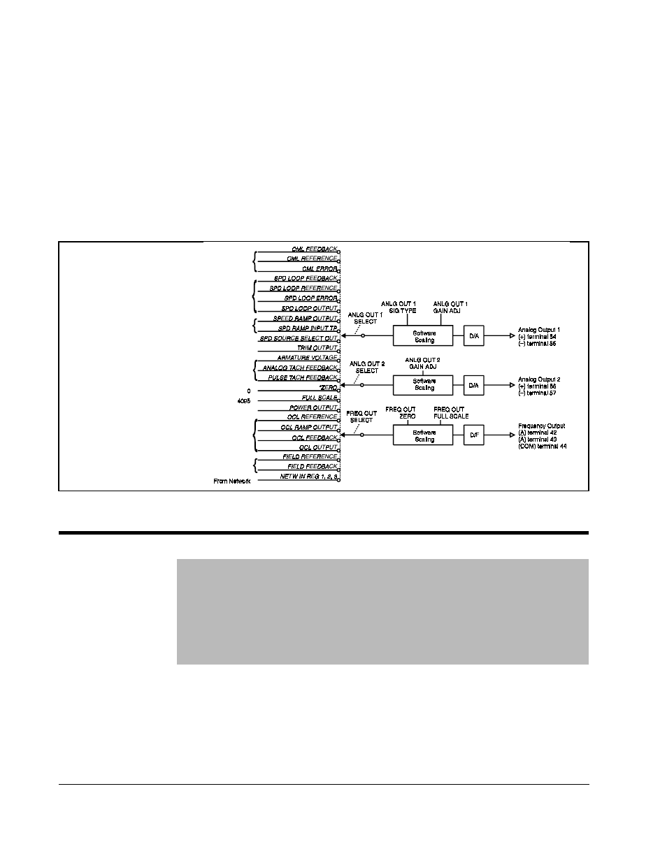
11.3 Configuring the Analog Outputs
The I/O Expansion kit has two unfiltered analog outputs. One can generate a bipolar
DC voltage only. The other can be configured to generate a DC voltage from a 0 to
±
10 VDC, 4-20 mA, or 10-50 mA signal. These outputs can be scaled to generate DC
voltage signals as low as 5 V, but maximum resolution (0.025%) is obtained when the
full scale output signal is used. The full scale value (
FSV
) is determined based on the
selected parameter group; load, speed, voltage, power, field or other.
Analog outputs are read every 5msec when
FEEDBACK
SELECT
(P.200) is set to
DC
TACH
,
PULSE
TACH
, or
AC
TACH
. They are read every 10 msec when
FEEDBACK
SELECT
(P.200) is set to
ARMATURE
VOLT
.
Figure 11.3 – Analog and Frequency Outputs Block Diagram
ANLG
OUT
1
GAIN
ADJ
(P.420)
Adjusts the gain of
analog output 1
(terminals 54 and 55
of the I/O Expansion
kit) to allow it to
produce a signal from
5.0 to approximately
13.0VDC.
Parameter Range:
0.500 to 1.300
Default Setting:
1.000
Parameter Type:
Tunable
OIM Menu Path(s):
Input/Output - Analog I/O
The full scale value is determined by
ANLG
OUT
1
SELECT
. See table 11.1.
This parameter is typically used to adjust the 10 V full scale output to match the
input voltage requirement of attached equipment. For example, you would set this
parameter to 0.800 for equipment that accepts a 0 to 8 VDC signal.
Analog output 1 and 2 are only rated to 10 VDC, so gain adjustment values greater
than 1.000 might cause the analog output circuit to saturate.
From Figure 6.2,
Current Minor
Loop Block Diagram
From Figure 5.1,
Speed Loop
Block Diagram
From Figure 4.5,
Speed Reference
Ramp Block Diagram
From Figure 4.2,
Speed Reference Source Select Block Diagram
From Figure 9.1,
Outer Control
Loop Block Diagram
From Figure 8.1,
Field Block DIagram if Field
Current Regulator Kit is Installed
From Figure 5.1,
Speed Loop Block Diagram
From Figure 4.5,
Speed Reference Ramp Block Diagram
See table 11.1 on page 11-12
*Default Selection