Figure 6-4. port ram indirect access – Rainbow Electronics DS31256 User Manual
Page 53

DS31256
53 of 181
Register Name:
CP[n]RD, where n = 0 to 15 for each port
Register Description: Channelized Port [n] Register Data
Register Address:
See the Register Map in Section
Bit
# 7 6 5 4 3 2 1 0
Name CHD7 CHD6 CHD5 CHD4 CHD3 CHD2 CHD1 CHD0
Default 0 0
0
0
0
0
0
0
Bit
# 15 14 13 12 11 10 9 8
Name
CHD15 CHD14 CHD13 CHD12 CHD11 CHD10 CHD9 CHD8
Default 0
0
0
0
0
0
0
0
Note: Bits that are underlined are read-only; all other bits are read-write.
Bits 0 to 15/DS0 Channel Data (CHD0 to CHD15). This is the 16-bit data that is to either be written into or read
from the PORT RAM, specified by the CP[n]RDIS register.
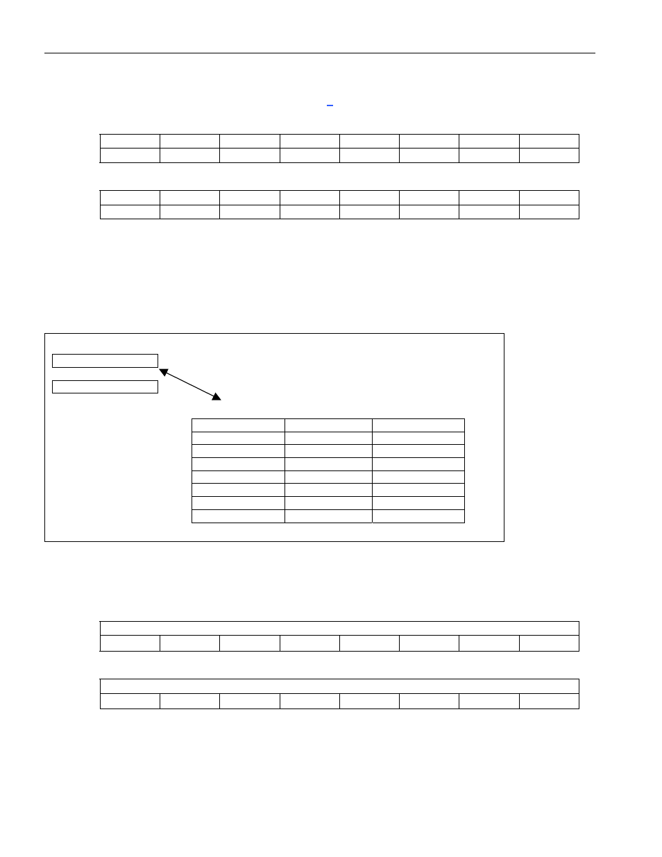
Figure 6-4. Port RAM Indirect Access
CP[n]RDIS
CP[n]RD
Port RAM (one each for all 16 ports; n = 0 to 15)
C[n]DAT0 R[n]CFG0 T[n]CFG0
C[n]DAT1 R[n]CFG1 T[n]CFG1
C[n]DAT2 R[n]CFG2 T[n]CFG2
C[n]DAT3 R[n]CFG3 T[n]CFG3
C[n]DAT4 R[n]CFG4 T[n]CFG4
... ... ...
C[n]DAT126 R[n]CFG126 T[n]CFG126
C[n]DAT127 R[n]CFG127 T[n]CFG127
Register Name:
C[n]DAT[j], where n = 0 to 15 for each port and j = 0 to 127 for each DS0
Register Description: Channelized Layer 1 DS0 Data Register
Register Address:
Indirect Access through CP[n]RD
Bit
# 7 6 5 4 3 2 1 0
Name
RDATA(8): Receive DS0 Data
Default
Bit
# 15 14 13 12 11 10 9 8
Name
TDATA(8): Transmit DS0 Data
Default
Note: Bits that are underlined are read-only; all other bits are read-write.
Note: In normal device operation, the host must never write to the C[n]DAT[j] registers.
Bits 0 to 7/Receive DS0 Data (RDATA). This register holds the most current DS0 byte received. It is used by the
transmit side Layer 1 state machine when channelized network loopback (CNLB) is enabled.
