Pci write cycle, Figure 10-3. pci bus write, 2 pci write cycle – Rainbow Electronics DS31256 User Manual
Page 132

DS31256
132 of 181
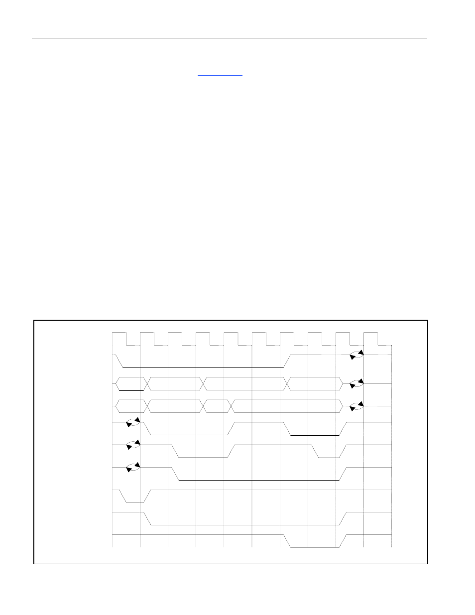
10.1.2 PCI Write Cycle
A write cycle on the PCI bus is shown in
. During clock cycle #1, the initiator asserts the
PFRAME signal and drives the address onto the PAD signal lines and the bus command (which would be
a write) onto the PCBE signal lines. The target reads the address and bus command and, if the address
matches its own, it then asserts the PDEVSEL signal and begins the bus transaction. During clock cycle
#2, the initiator stops driving the address onto the PAD signal lines and begins driving data #1. It also
switches the PCBE signal lines to indicate the byte enable for data #1. The initiator asserts the PIRDY
signal and begins monitoring the PDEVSEL and PTRDY signals. During clock cycle #3, the initiator
detects that PDEVSEL and PTRDY are asserted, which indicates that the target has accepted data #1 and
the initiator begins driving the data and byte enable for data #2. During clock cycle #4, since PDEVSEL
and PTRDY are asserted, data #2 is written by the initiator to the target. During clock cycle #5, both
PIRDY and PTRDY are deasserted, indicating that neither the initiator nor the target are ready for data #3
to be passed. During clock cycle #6, the initiator is ready so it asserts PIRDY and deasserts PFRAME,
which indicates that data #3 is the last one passed. During clock cycle #8, the target asserts PTRDY,
which indicates to the initiator that data #3 is ready to be accepted by the target. During clock cycle #9,
the initiator deasserts PIRDY and stops driving the PAD and PCBE signal lines. The target deasserts
PDEVSEL and PTRDY.
The PXAS, PXDS, and PXBLAST signals are not part of a standard PCI bus. These PCI extension
signals are unique to the device. They are useful in adapting the PCI bus to a proprietary bus scheme.
They are only asserted when the device is a bus master.
Figure 10-3. PCI Bus Write
1
2
3
4
5
6
7
8
9
10
data #1
Address
CMD
BE #1
PCLK
PFRAME
PAD
PCBE
PIRDY
PTRDY
PDEVSEL
PXDS
PXAS
PXBLAST
data #2
data #3
BE #2
BE #3
