Pci read cycle, Figure 10-2. pci bus read, 1 pci read cycle – Rainbow Electronics DS31256 User Manual
Page 131

DS31256
131 of 181
10.1.1 PCI Read Cycle
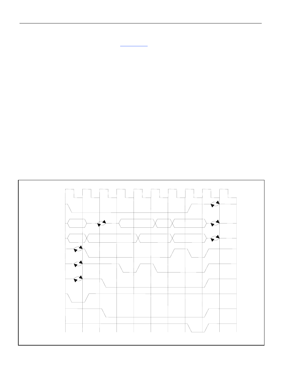
A read cycle on the PCI bus is shown in
. During clock cycle #1, the initiator asserts the
PFRAME signal and drives the address onto the PAD signal lines and the bus command (which would be
a read) onto the PCBE signal lines. The target reads the address and bus command and, if the address
matches its own, it then asserts the PDEVSEL signal and begins the bus transaction. During clock cycle
#2, the initiator stops driving the address onto the PAD signal lines and switches the PCBE signal lines
to indicate byte enables. It also asserts the PIRDY signal and begins monitoring the PDEVSEL and
PTRDY signals. During clock cycle #4, the target asserts PTRDY, indicating to the initiator that valid
data is available to be read on the PAD signal lines by the initiator. During clock cycle #5, the target is
not ready to provide data #2 because PTRDY is deasserted. During clock cycle #6, the target again
asserts PTRDY, informing the initiator to read data #2. During clock cycle #7, the initiator deasserts
PIRDY, indicating to the target that it is not ready to accept data. During clock cycle #8, the initiator
asserts PIRDY and acquires data #3. Also during clock cycle #8, the initiator deasserts PFRAME,
indicating to the target that the bus transaction is complete and no more data needs to be read. During
clock cycle #9, the target deasserts PTRDY and PDEVSEL and the initiator deasserts PIRDY.
The PXAS, PXDS, and PXBLAST signals are not part of a standard PCI bus. These PCI extension
signals are unique to the device and are useful in adapting the PCI bus to a proprietary bus scheme. They
are only asserted when the device is a bus master.
Figure 10-2. PCI Bus Read
1
2
3
4
5
6
7
8
9
10
data #3
Address
CMD
Byte Enable #1
PCLK
PFRAME
PAD
PCBE
PIRDY
PTRDY
PDEVSEL
PXDS
PXAS
PXBLAST
data #1
data #2
BE #2
BE #3
