Test register description, Egister, Escription – Rainbow Electronics DS31256 User Manual
Page 43: 4 test register description
DS31256
43 of 181
Bit 13/Status Bit for Transmit DMA Pending-Queue Read (TPQR)
0 = interrupt masked
1 = interrupt unmasked
Bit 14/Status Bit for Transmit DMA Done-Queue Write (TDQW)
0 = interrupt masked
1 = interrupt unmasked
Bit 15/Status Bit for Transmit DMA Done-Queue Write Error (TDQWE)
0 = interrupt masked
1 = interrupt unmasked
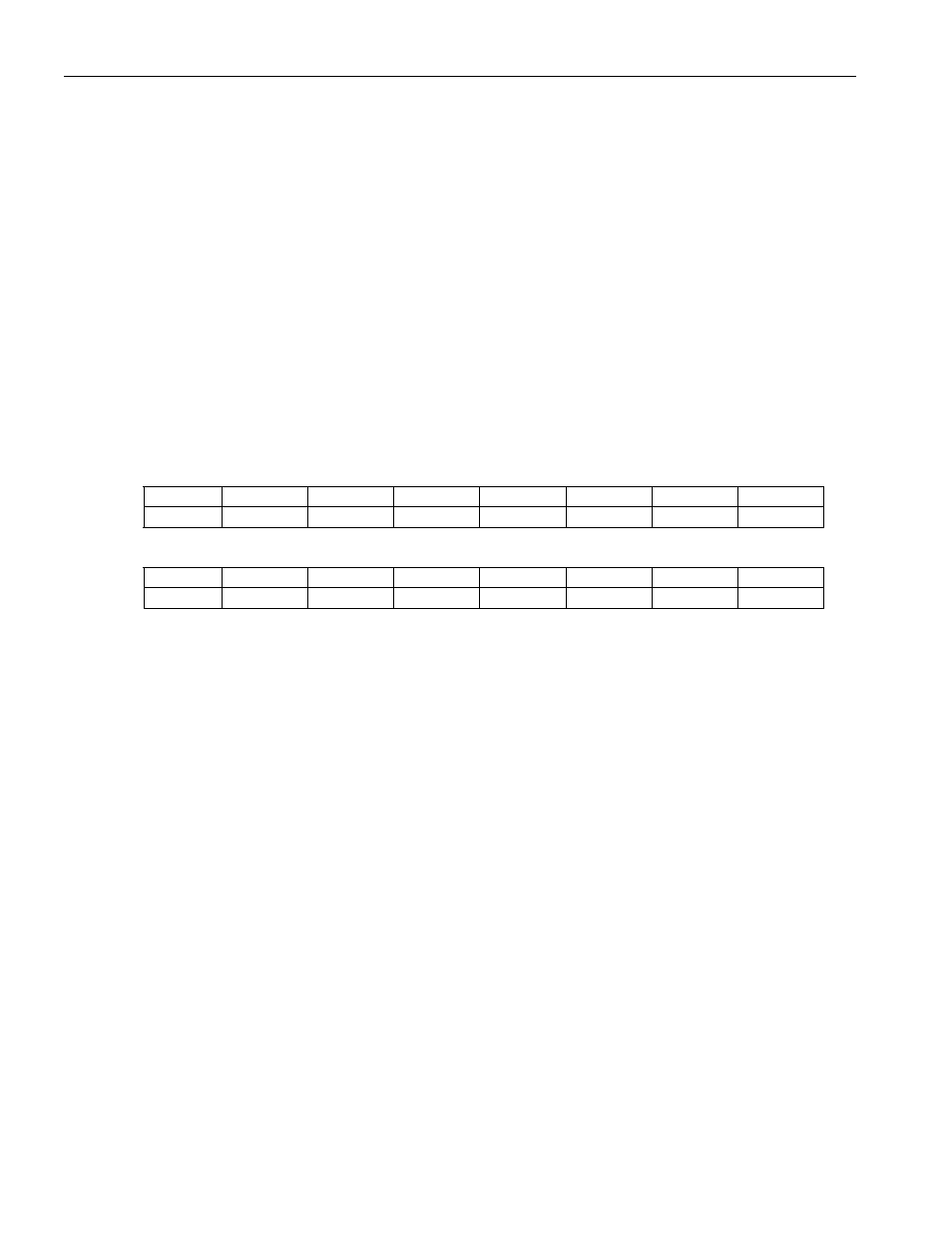
5.4 Test Register Description
Register Name:
TEST
Register Description: Test Register
Register Address:
0050h
Bit
# 7 6 5 4 3 2 1 0
Name n/a n/a
n/a
n/a
n/a
n/a
n/a
FT
Default
0 0 0 0 0 0 0 0
Bit
# 15 14 13 12 11 10 9 8
Name n/a
n/a
n/a
n/a
n/a
n/a
n/a
n/a
Default
0 0 0 0 0 0 0 0
Note: Bits that are underlined are read-only; all other bits are read-write.
Bit 0/Factory Test (FT). This bit is used by the factory to place the DS31256 into the test mode. For normal
device operation, this bit should be set to 0 whenever this register is written to. Setting this bit places the RAMs
into a low-power standby mode.
Bit 1 to 15/Device Internal Test Bits. Bits 1 to 15 are for internal (Dallas Semiconductor) test use only, not user
test-mode controls. Values of these bits should always be 0. If any of these bits are set to 1 the device does not
function properly.