Register address field definitions (load format) – Avago Technologies LSI53C1010 User Manual
Page 79
Instruction Descriptions
3-39
Description
The Load instruction is more efficient than a Move Memory instruction
when moving data from a memory location to an internal register of the
chip. It is a two Dword instruction, compared to three Dwords for a
Memory Move. This instruction may be used to move up to 4 bytes. The
number of bytes being loaded is indicated by the low order bits in the first
Dword of the instruction. The maximum number of bytes is defined by
the Register Address field, as illustrated in
Notes
The register address and memory address must have the same byte
alignment, and the byte count set so that it does not cross Dword
boundaries. The memory address may not map back to the SCRIPTS
processor operating registers, although it may map back to a location in
the SCRIPTS RAM. If these conditions are violated, a PCI illegal
read/write cycle will occur and the chip will issue an Interrupt (Illegal
Instruction Detected) immediately following, because the intended
operation did not happen.
Loads from SCRIPTS RAM cross the PCI bus, except for the
LSI53C896/10XX chips. However, it is selectable for debug.
Load/Store
This field defines whether the instruction will be executed as a
Load or a Store.
0 - Store instruction
1 - Load instruction
Register
Address
These bits select the register to load within the chip operating
register set.
Byte Count
Indicates the number of bytes to transfer. Valid values are 1, 2,
3, or 4.
Source
Address
Actual address (or offset from the DSA) of the data to load into
the chip register.
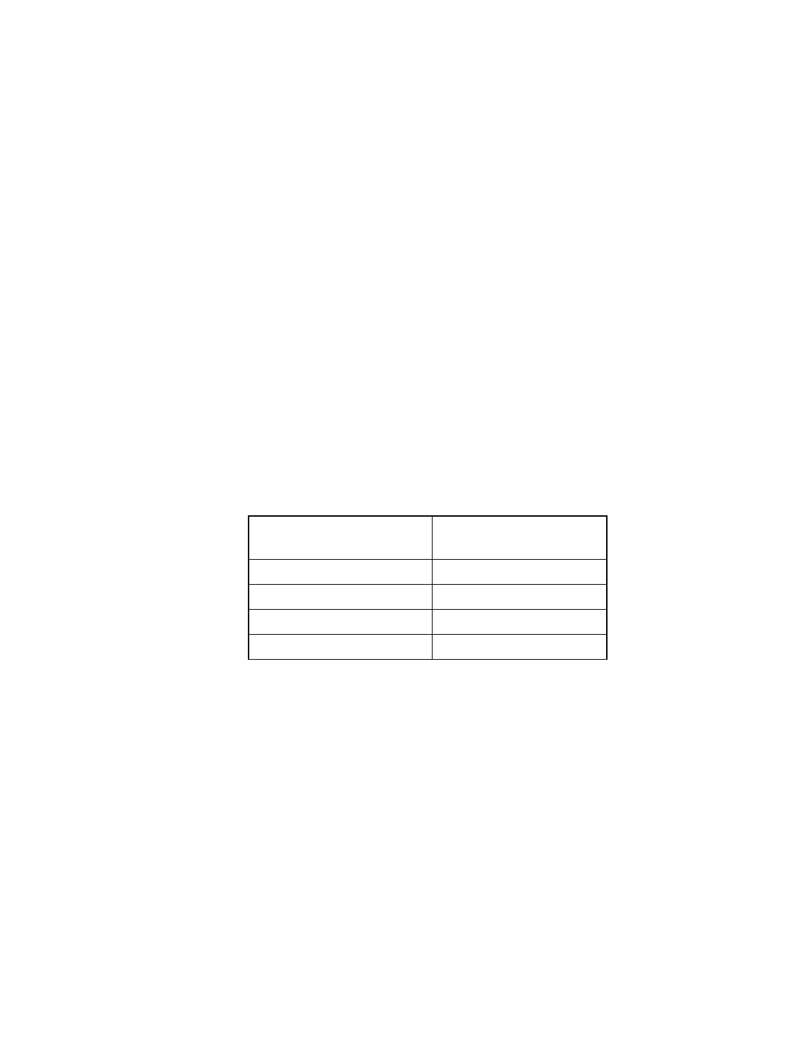
Table 3.10
Register Address Field Definitions (LOAD Format)
DBC Bits [17:16]
(Register Address bits A1:A0)
Number of Bytes to Load
00
1, 2, 3, or 4
01
1, 2, or 3
10
1 or 2
11
1