2 larger fifo, 3 new istat registers, Table 13.1 istat1 register – Avago Technologies LSI53C1010 User Manual
Page 272: 4 new scratch registers, 5 new load/store feature, Larger fifo, New istat registers, New scratch registers, New load/store feature, Istat1 register
13-2
New SCRIPTS Processor Features
13.2 Larger FIFO
FIFO size varies with the specific chip. Refer to
for specifics.
Max burst size is now 64 levels in the LSI53C896/10XX due to the
increased FIFO width.
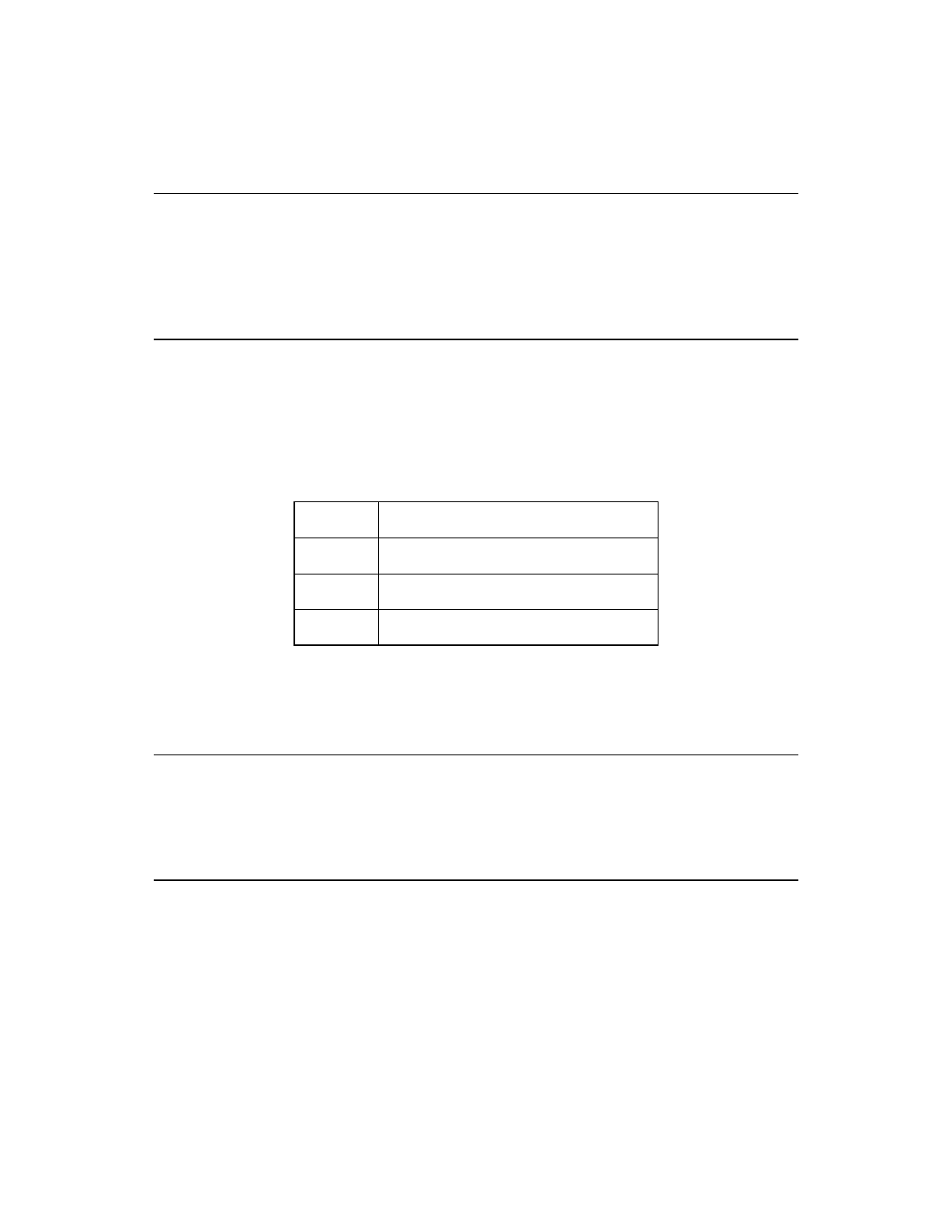
13.3 New ISTAT Registers
ISTAT for these chips is now 32-bits wide. ISTAT1 is in byte lane 1. For
more details on ISTAT registers, refer to the appropriate chip technical
manual.
provides an overview of the registers in ISTAT1.
Byte lane 2 and 3 are general purpose mailbox registers (MBOX1 and
MBOX2) that communicate with the SCRIPTS engine. All 8 bits of a
mailbox should be either writes or reads, not a combination.
13.4 New Scratch Registers
Eight new 32-bit Scratch registers have been added to the chips, for a
total of 18. The new registers are SCRATCHK through SCRATCHR.
13.5 New Load/Store Feature
The SCRIPTS processor no longer uses the PCI bus for Load/Store
instructions when moving data between the chip registers and the
SCRIPTS RAM. This feature can be disabled by setting bit 1 of CCNTL0
(Offset 0x56).
Table 13.1
ISTAT1 Register
Bits [7:3]
Reserved
Bit 2
Flushing in progress
Bit 1
SCRIPTS running
Bit 0
Synchronous IRQ disable