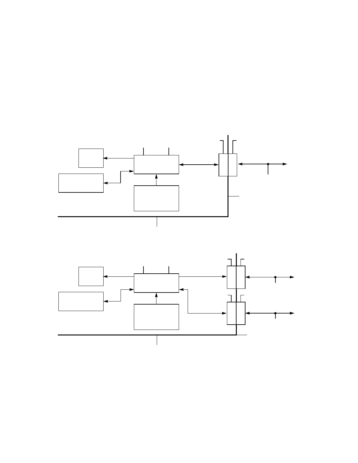
Figure1.1 single channel block diagram, Figure1.2 dual channel block diagram, Single channel block diagram – Avago Technologies LSI53C1010 User Manual
Page 26: Dual channel block diagram

1-6
Using the Programming Guide
manual in order to effectively program SCRIPTS for each
chip.
Figures 1.1
and
are block diagrams of the single and dual channel
LSI Logic chips that support SCRIPTS, with a map of SCSI data and
control paths through the chips.
Figure 1.1
Single Channel Block Diagram
Figure 1.2
Dual Channel Block Diagram
PCI Bus
External Memory
Single
External Oscillator
or Optimal Internal
Connection to
PCI Bus Clock
VDD
VSS
Peripheral
SCLK
SCSI Term Connection
SCSI Connection
SCSI Bus
(When Supported)
CPU Box
Bulkhead
CPU baseboard
Channel Chip
PCI Bus
External Memory
Dual
External Oscillator
or Optimal Internal
Connection to
PCI Bus Clock
VDD
VSS
Peripheral
SCLK
SCSI Term Connection
SCSI Connection
SCSI Bus
(When Supported)
CPU Box
Bulkhead
CPU baseboard
Channel Chip
SCSI Term Connection
SCSI Connection
SCSI Bus
Peripheral
