Table 6.6 phase mismatch registers, 8 test and miscellaneous registers, Test and miscellaneous registers – Avago Technologies LSI53C1010 User Manual
Page 159: Phase mismatch registers
Test and Miscellaneous Registers
6-9
6.8 Test and Miscellaneous Registers
The test registers are used to test the DMA and SCSI FIFOs and perform
other miscellaneous functions. The test registers are listed in
Test registers can be used to decrement the byte count or increment the
address count in the FIFOs.
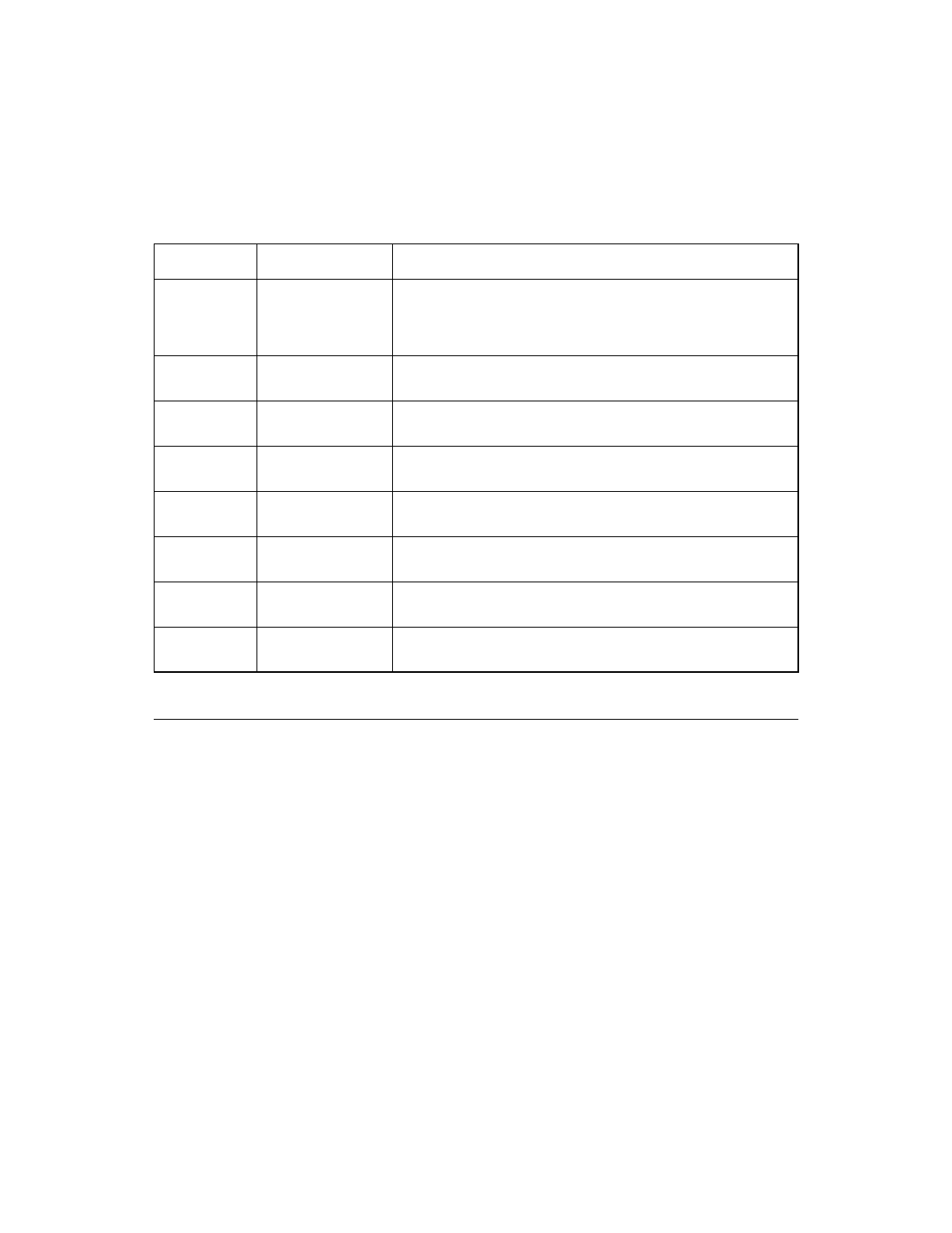
Table 6.6
Phase Mismatch Registers
Name
Definition
Functions
CCNTL0
Chip Control 0
Various JUMP control functions, Disable Auto-FIFO Clear,
Disable Internal Load/Store (LSI53C89X only), Disable Internal
SCRIPTS RAM Cycles, Disable Pipe Request (LSI53C10XX
only).
CSBC
Cumulative SCSI
Byte Count
Cumulative byte count of data transferred across the SCSI bus
during data phases.
ESA
Entry Storage
Address
Contains BMOV instruction address information.
IA
Instruction Address
Contains the address of the BMOV instruction that was
executing at the time of a phase mismatch.
PMJAD (1, 2)
1
1. LSI53C10XX only.
Phase Mismatch
Jump Address
Contains the address that will be jumped to in the case of a
phase mismatch. PMJAD is outbound, PMJAD2 is inbound.
RBC
Remaining Byte
Count
Byte count that remains for the BMOV instruction that was
executing at the time of a phase mismatch.
SBC
SCSI Byte Count
Number of bytes transferred to or from the SCSI bus during any
given BMOV.
UA
Updated Address
Contains the updated data address of the BMOV that was
executing at the time of a phase mismatch.