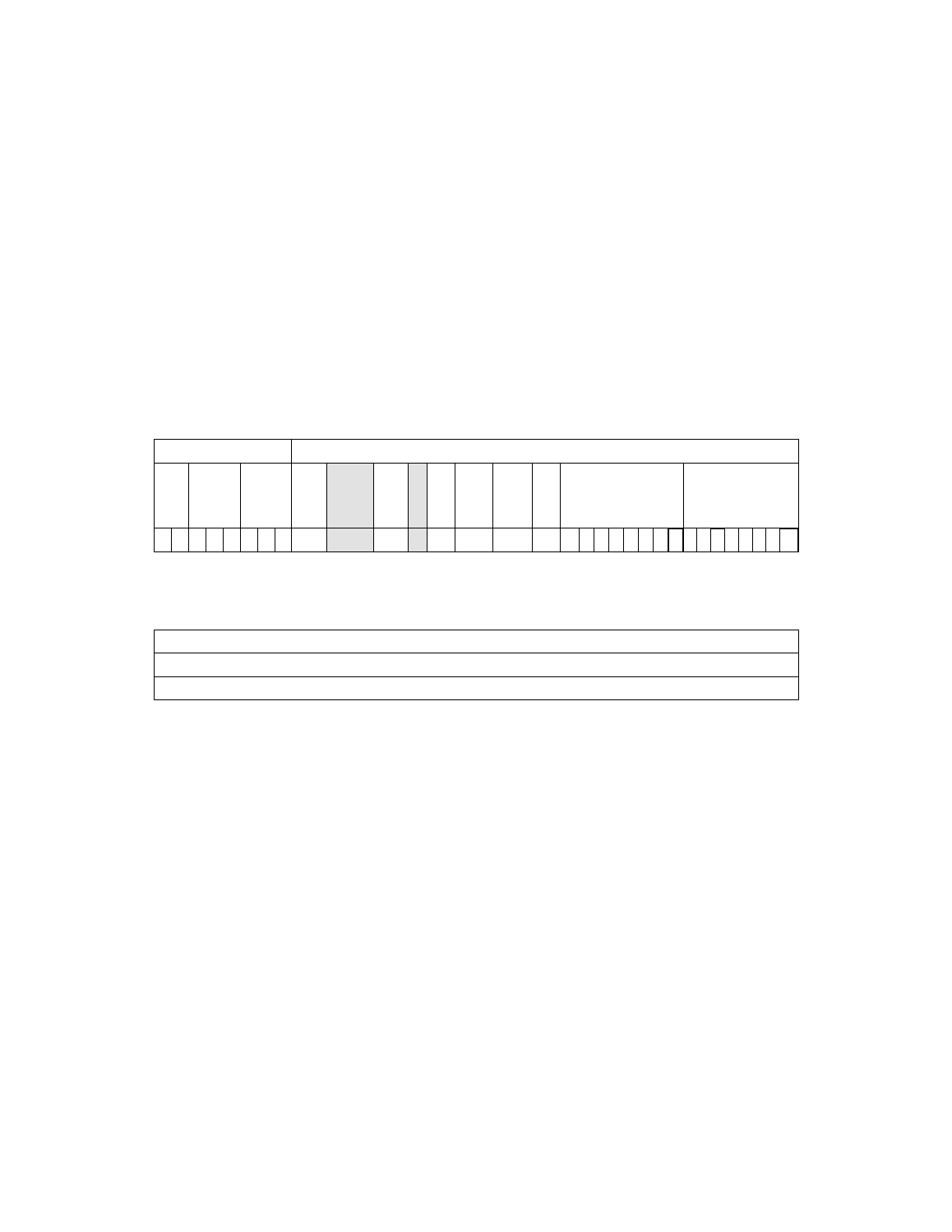
Figure3.1 call format, Call format – Avago Technologies LSI53C1010 User Manual
Page 46

3-6
The SCSI SCRIPTS Processor Instruction Set
Example
CALL REL (Address), WHEN DATA_OUT
Field(s)
This command has the following fields:
The values in
define the SCSI information transfer phase. The
LSI53C10XX chips, with dual transition timing capabilities define two
transfer phases, ST for single transition timing, and DT for dual transition
timing.
MASK
Represents an 8-bit value that is stored in the mask field of the
instruction when this field is present. Any bit that is set in the
mask causes the corresponding bit in the data byte to be
ignored at the time of the comparison.
CARRY
Indicates that a jump should take place based on the value of
the carry bit in the ALU. Carry comparisons cannot take place
at the same time as data and phase comparisons.
Figure 3.1
CALL Format
31 30 29
27 26
24
23
22
21
20 19
18
17
16 15
8 7
0
DCMD Register
DBC Register
Instr
Type
Opcode
SCSI
Phase
Real
Addr
Mode
R
1
64-bit
jump
enable
2
1. All chips except LSI53C10XX.
2. LSI53C10XX chips.
Carry
Test
R True
Comp
Data
Comp
Phase
Wait
Mask
Data
1 0 0 0 1 x x x
x
0
0
0
x
x
x
x
x x x x x x x x x x x x x x x x
31
0
DSPS Register
Call Address or Offset
Call Address
Opcode
Transfer Control Instruction, Call subroutine.
SCSI Phase
These bits reflect the actual values of the SCSI phase lines.
