3 dma registers, Dma registers – Avago Technologies LSI53C1010 User Manual
Page 154
6-4
Using the Registers to Control Chip Operations
6.3 DMA Registers
lists the DMA registers. The DMA registers are used for the
following functions:
•
Setting up the host interface.
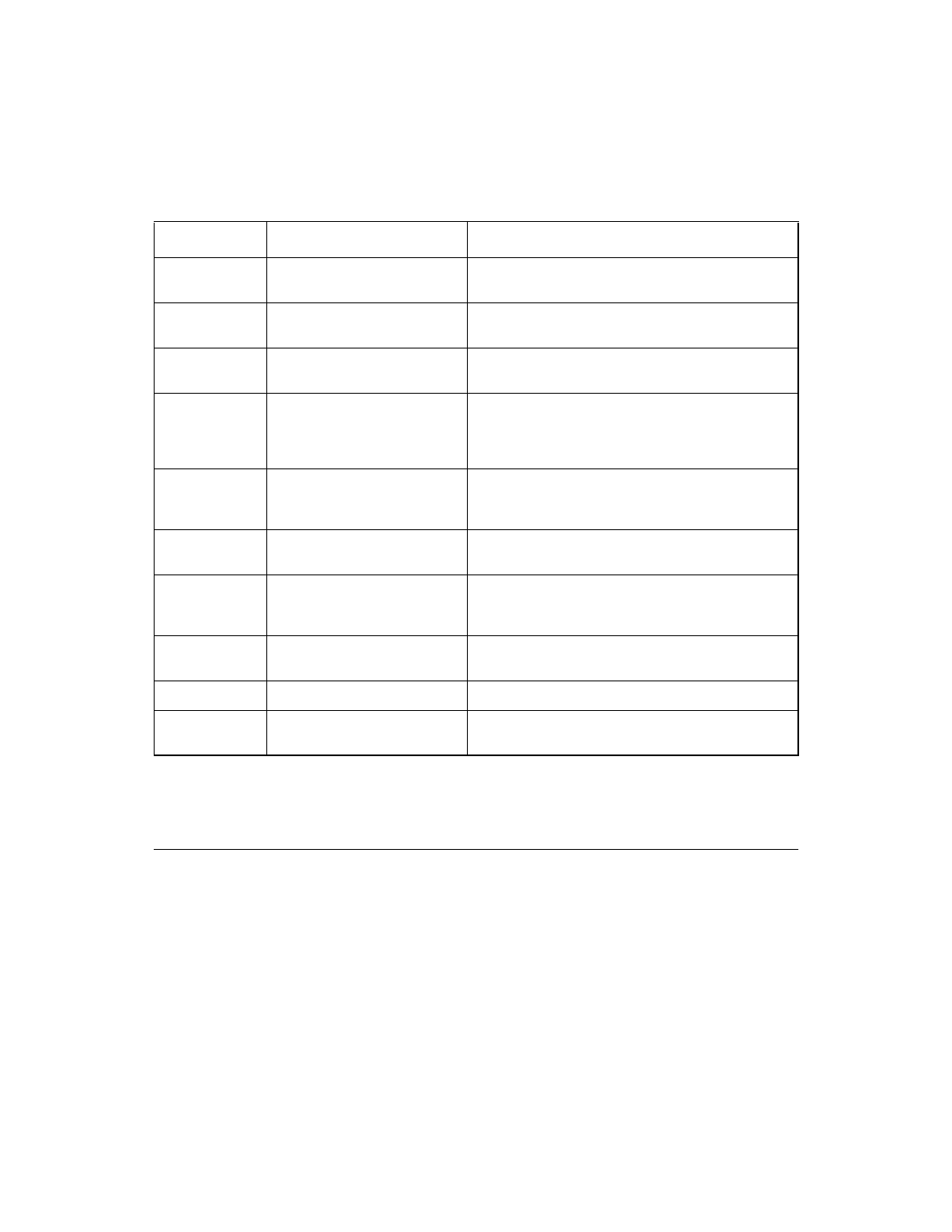
SSTAT1
SCSI Status 1
FIFO flags; latched SCSI parity signal; latched
SCSI phase status bits.
SSTAT2
SCSI Status 2
Reports SIDL, SODR, SODL most significant byte
full; parity detection, disconnect detection.
STEST0
SCSI Test 0
These bits are used for low level operation and
manufacturing testing, SCSI selected as ID.
STEST1
SCSI Test 1
Disable the external SCLK pin and use the PCI
clock as the internal SCSI clock; enable the SCSI
Clock doubler (LSI53C825A/875/876/885 only) or
SCSI clock quadupler (LSI53C895/896/10XX only).
STEST2
SCSI Test 2
Clear synchronous offset; Enable Differential Mode;
wide SCSI; extend SREQ/–SACK/ filtering; Low
Level Mode enable.
STEST3
SCSI Test 3
Active negation enable; SCSI FIFO test read/write;
Halt SCSI clock; Clear SCSI FIFO.
STEST4
4
SCSI Test 4
Contains DIFFSENS pin values that indicate the
type of SCSI device connected to the bus;
frequency lock bit for clock quadrupler.
STIME0
SCSI Timer 0
Selects the handshake-to-handshake time-out
period.
STIME1
SCSI Timer 1
Selects the general purpose time-out period.
SXFER
SCSI Transfer
Define synchronous transfer period and
synchronous offset.
1. Wide SCSI products only.
2. LSI53C10XX only.
3. LSI53C895 and later.
4. LSI53C895A and later only.
Table 6.1
SCSI Registers (Cont.)
Name
Definition
Functions