Avago Technologies LSI53C1010 User Manual
Page 22
1-2
Using the Programming Guide
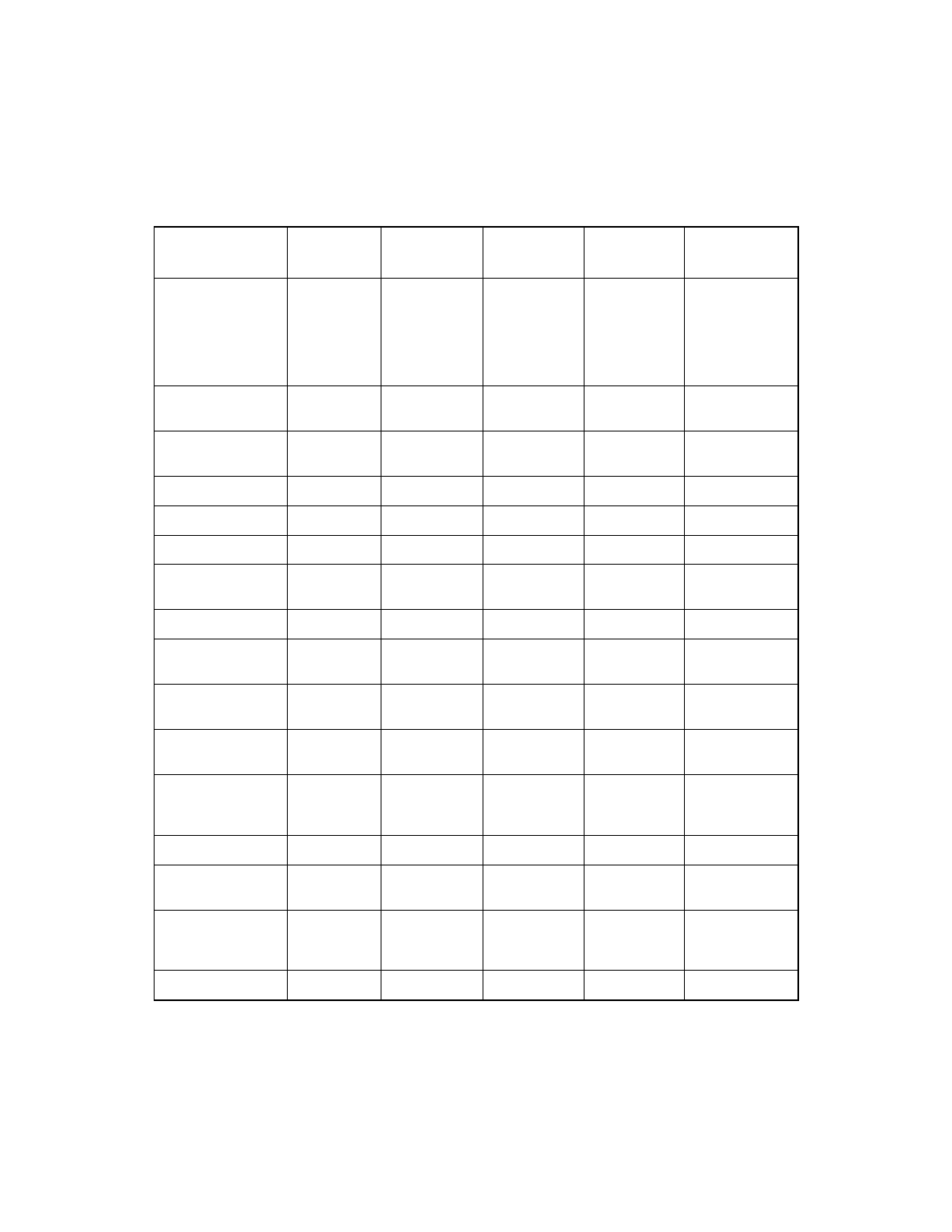
Table 1.1
Features and Functions of LSI53C7XX/8XX/10XX Family Chips (part 1)
LSI53C770
LSI53C810A
LSI53C860
LSI53C815
LSI53C825A
LSI53C825AJ
Maximum Transfer
Rate
20 Mbytes/s
synchronous
(with Wide
SCSI)
5 Mbytes/s
asynchronous
10 Mbytes/s
synchronous
5 Mbytes/s
asynchronous
20 Mbytes/s
synchronous
(with Ultra
SCSI)
5 Mbytes/s
asynchronous
10 Mbytes/s
synchronous
10 Mbytes/s
asynchronous
20 Mbytes/s
synchronous
DMA FIFO Size
(bytes)
96
80
80
64
88 or 536
Synchronous
Offset (levels)
16
8
8
8
16
SCRIPTS RAM
4 Kbytes
None
None
None
4 Kbytes
Differential SCSI
No
No
No
No
HVD
Wide SCSI
Yes
No
No
No
Yes
External Memory
Interface
No
No
No
Yes
Yes
Instruction Prefetch Yes
Yes
Yes
No
Yes
Load/Store
Instructions
No
Yes
Yes
No
Yes
Enhanced Move
Register Capability
No
No
No
No
Yes
SCSI Selected As
ID Bits
No
Yes
Yes
No
Yes
Number of 32-bit
SCRATCH
Registers
1
2
2
2
10
PCI Caching
No
Yes
Yes
No
Yes
Selectable IRQ
Disable
No
Yes
Yes
No
Yes
Big/Little Endian
Support
Big or Little
Endian
Little Endian
Little Endian
Big or Little
Endian
Big or Little
Endian (except
LSI53C825AJ)
PCI Data Bus
N/A
32-Bit
32-Bit
32-Bit
32-Bit