Table 6.7 test and miscellaneous registers, Test and miscellaneous registers – Avago Technologies LSI53C1010 User Manual
Page 160
6-10
Using the Registers to Control Chip Operations
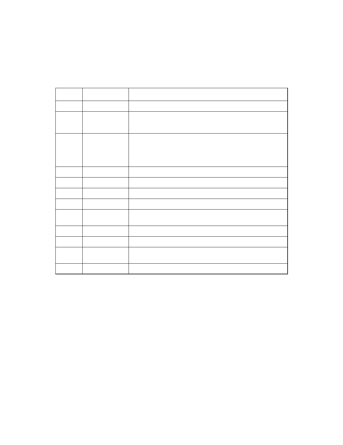
Table 6.7
Test and Miscellaneous Registers
Name
Definition
Functions
ADDER
Adder Sum Output Contains output of internal adder.
CCNTL0
1
Chip Control 0
Various JUMP control functions, Disable Auto FIFO Clear, Disable
Internal Load/Store (LSI53C89X only), Disable Internal SCRIPTS
RAM Cycles (LSI53C10XX only), Disable Pipe Request
CCNTL1
1
Chip Control 1
Disable DAC, 64-Bit Table Indirect Indexing Mode, Enable 64-Bit
Table Indirect BMOV, Enable 64-Bit Direct BMOV
LSI53C89X only: High Impedance Mode
LSI53C10XX only: Pull Enable, Pull Disable, Disable 64-Bit Master
Operation, Disable 64-Bit Slave Cycles.
CCNTL2
2
Chip Control 2
Reserved.
CCNTL3
2
Chip Control 3
Skew Control, LVD Drive Strength Control.
CTEST0
Chip Test 0
Used to enable power management modes in the LSI53C885.
CTEST1
Chip Test 1
DMA FIFO bits full or empty.
CTEST2
Chip Test 2
Data transfer direction; I/O or memory configuration;
request/acknowledge status.
CTEST3
Chip Test 3
Revision level bits, flush/clear DMA FIFO.
CTEST4
Chip Test 4
Burst disable; master parity error enable; DMA FIFO byte control.
CTEST5
Chip Test 5
Clock address incrementor; clock byte counter; DMA direction;
control of set or reset pulses.
CTEST6
Chip Test 6
Writes data to the DMA FIFO.
1. LSI53C895 and later only.
2. LSI53C10XX only.