Figure3.28 transfer control instruction, 4 read/write instruction example, Read/write instruction example – Avago Technologies LSI53C1010 User Manual
Page 117: Transfer control instruction, Figure 3.28 transfer control instruction
Instruction Examples
3-77
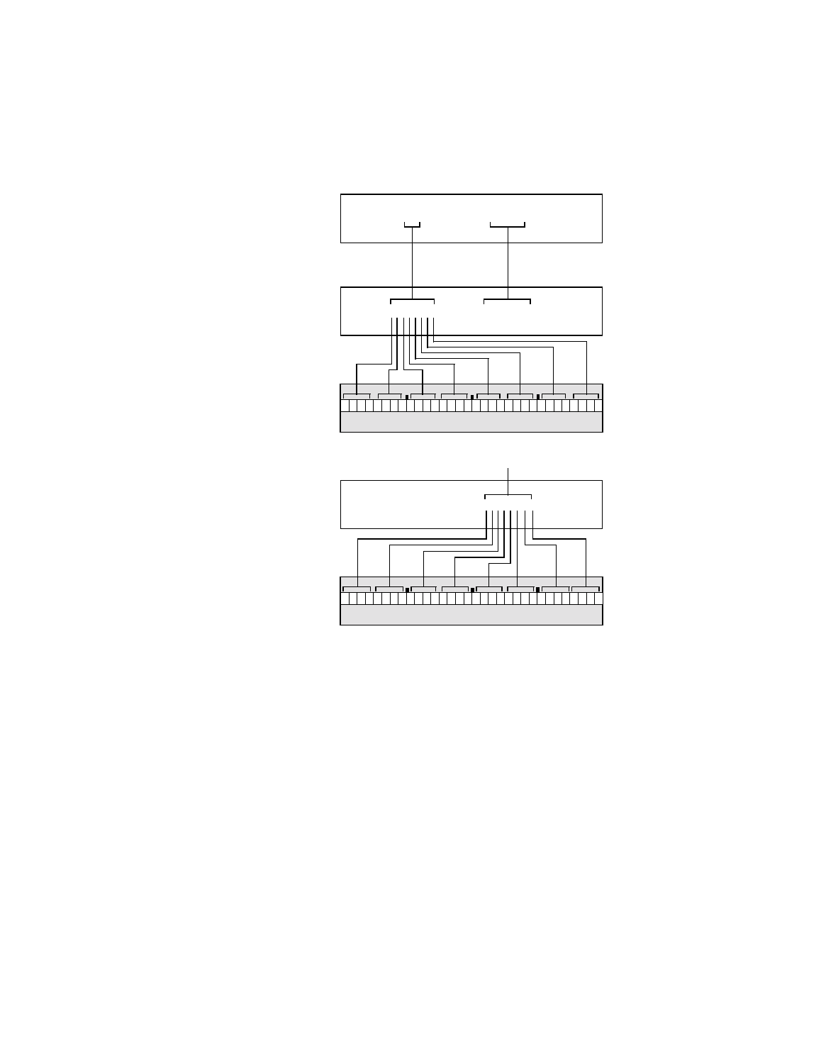
Figure 3.28 Transfer Control Instruction
3.3.4 Read/Write Instruction Example
This example writes 0b01 into the SCSI Chip ID (SCID) register, as
shown in
. This is illustrated by the translation of the
hexadecimal compiler output into binary format.
The MOVE instruction is 78 in hexadecimal, translating into 0b01 for
Read/Write; 0b111, the opcode for the Read/Modify/Write function; and
0b00 in the operator field to indicate that the instruction will operate on
the immediate data and write to the destination register. The address of
register SCID is 04 in hexadecimal, translating to a binary format for the
Register Address bits of the DBC register.
NASM
Output
0
0 0 0 0 0
0 0 0 0 0 0 0
0 0 0 0 1 0 1 0 1 1 0 0 1 0 1 1
0
0
0
Binary
Instruction
Format
DSPS Register
1
0 1 1 0 0
0 0 0 0 0 0 0
0 0 0 0 0 0 0 0 0 0 0 0 0 0 0
0
0
0
Binary
Instruction
Format
DCMD Register
DBC Register
98000000
00000ACB
(0xACB)
98000000
00000ACB
INT
0xACB
SCSI SCRIPTS
Source Code