Pid control block, Fig 6.63 pid control block – Yaskawa Matrix Converter User Manual
Page 265
6
-100
PID Control Block
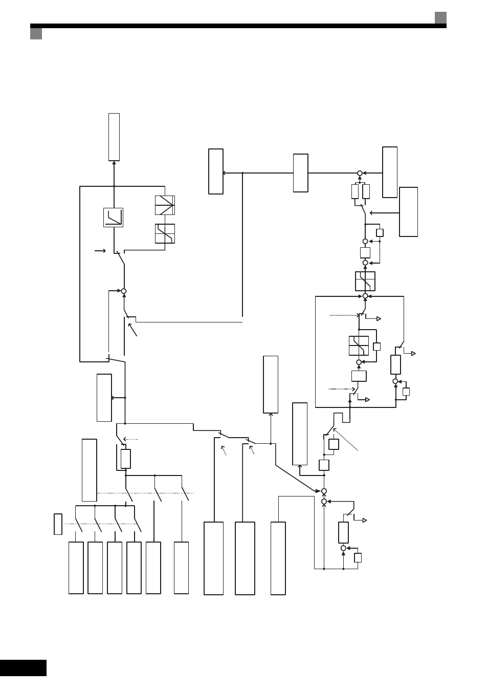
The following diagram shows the PID control block in the MxC.
Fig 6.63 PID Control Block
Option Card
Serial Com
Terminal A1
d1-01
d1-02
d1-16
Terminal A2 or A3 PID
target
v
al
u
e
MEMOBUS comm
u
nications
register 06 H PID target
v
al
u
e
Fre
qu
ency reference
terminal A3 PID feed
b
ack
Z
-1
b
5-03
+
−
+
P
b
1-01
0
1
2
3,4
Fre
qu
ency reference
u
sing m
u
lti-step command
PID Inp
u
t
V
ol
u
me
(U1-36)
Set PID target
v
al
u
e in
m
u
lti-f
u
nction analog inp
u
t
Set
b
it 1 of MEMOBUS
register 0FH to 1
b
5-01=2,4
b
5-01=1,3
Proportional
gain (P)
b
5-02
+
−
+
b
5-17
-1
Select m
u
lti-f
u
nction inp
u
ts
PID inp
u
t characteristics
PID SFS Cancel
H3-05 or
H3-09=B
O
u
tp
u
t fre
qu
ency
1
T
b
5-05
− T
1
-1
PID O
u
tp
u
t
Gain (
b
5-10)
Z
-1
Z
-1
Fre
qu
ency reference
(U1-01)
PID command (U1-3
8
)
Integral (I) time
b
5-03
Store integral
u
sing
m
u
lti-f
u
nction inp
u
ts
I limit
b
5-01=1,3
b
5-01=2,4
Deri
vati
ve
time
Integral reset
u
sing
m
u
lti-f
u
nction inp
u
ts
PID limit
b
5-06
PID Limit
PID Primary Delay
Time Constant
b
5-0
8
PID Offset
Adj
u
stment (
b
5-07)
Select PID O
u
tp
u
t
Le
v
el Selection
(b
5-09)
+
+
−
+
+
+
+
−
+
+
+
+
PID O
u
tp
u
t Monitor
(U1-37)
b
5-01=0
b
5-01=3,4
b
5-01=1,2
PID ON
PID OFF
M
u
lti-f
u
nction inp
u
t PID control cancel
signal is on. PID is off
u
nder the
follo
w
ing conditions:
b
5-01 = 0
D
u
ring JDG command inp
u
t
b
5-11=0
b
5-11=1
Ena
b
le/disa
b
le re
v
erse operation
w
hen PI o
u
tp
u
t is negati
v
e
Upper limit
Fmax x109%
Lo
w
er limit 0
Upp
w
er limit
Fmax x109%
Lo
w
er limit
-(Fmaxx109%)
+
+
0
+
1
1
Z
-1