1 power management mode timing, Ower, Anagement – Maxim Integrated High-Speed Microcontroller User Manual
Page 96: Odes, Table 7-b. crystal vs. mips comparison
High-Speed Microcontroller User’s Guide
Rev: 062210
96 of 176
The DS87C520 and DS87C530 incorporate a Status register (
;C5h) to prevent the device from
accidentally reducing the clock rate during the servicing of an external interrupt or serial port activity.
This register can be interrogated to determine if a high priority, low priority, or power-fail interrupt is in
progress, or if serial port activity is occurring. Based on this information the software can delay or reject a
planned change in the clock divider rate.
In addition, the DS87C520 and DS87C530 can operate from the internal ring oscillator during normal
operation, not only during the crystal warmup period.
summarizes the new control bits
associated with the power management features.
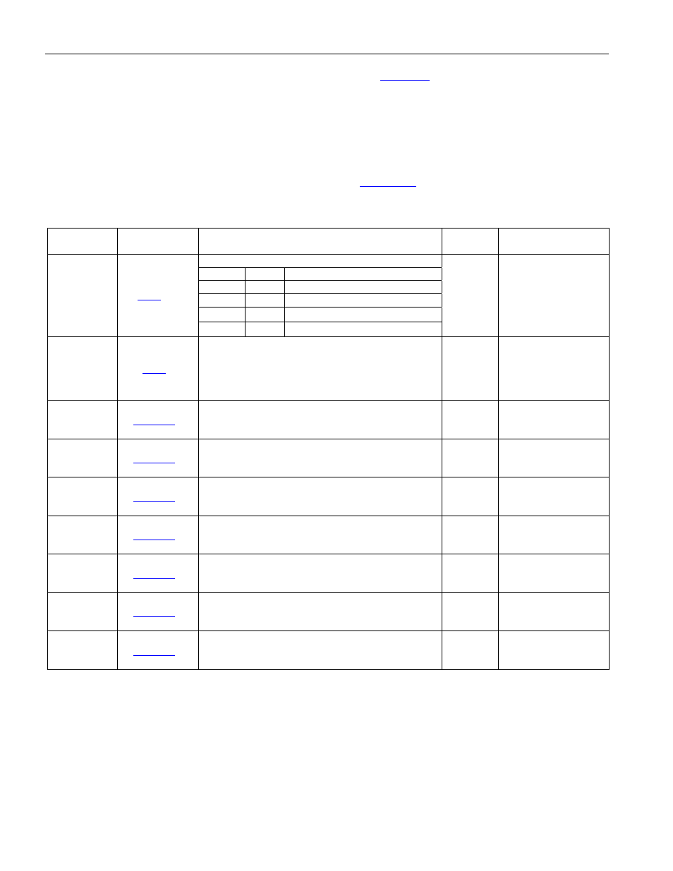
Table 7-C. Power Management and Status Bit Summary
BIT NAME
LOCATION
FUNCTION
RESET
STATE
READ/WRITE
ACCESS
Clock Divider Control
CD1
CD0
Osc Cycles per Machine Cycle
0
0
Reserved
0 1
4
(Reset
Default)
1 0
64
(PMM1)
CD1, CD0
.7-6
1 1
1024
(PMM2)
0,1
Write: 0,1 anytime;
1,0 and 1,1 only when
previously in 0,1
state. Unrestricted
read.
SWB
Switchback Enable
0 = Interrupts and serial port activity will not affect
clock divider control bits
1 = Enabled Interrupts and serial port activity will
cause a switchback
0 Unrestricted
PIP
Power-Fail Interrupt Status
0 = No power-fail interrupt in progress
1 = Power-fail interrupt in progress
0 Read
Only
HIP
High Priority Interrupt Status
0 = No high priority interrupt in progress
1 = High priority interrupt in progress
0 Read
Only
LIP
Low Priority Interrupt Status
0 = No low priority interrupt in progress
1 = Low priority interrupt in progress
0 Read
Only
SPTA1
Serial Port 1 Transmitter Activity Status
0 = Serial port 1 transmitter inactive
1 = Serial port 1 transmitter active
0 Read
Only
SPRA1
Serial Port 1 Receiver Activity Status
0 = Serial port 1 receiver inactive
1 = Serial port 1 receiver active
0 Read
Only
SPTA0
Serial Port 0 Transmitter Activity Status
0 = Serial port 0 transmitter inactive
1 = Serial port 0 transmitter active
0 Read
Only
SPRA0
Serial Port 0 Receiver Activity Status
0 = Serial port 0 receiver inactive
1 = Serial port 0 receiver active
0 Read
Only
7.3.1 Power Management Mode Timing
The two power management modes reduce power consumption by internally dividing the clock signal to
the device, causing it to operate at a reduced speed. When PMM is invoked, the external crystal will
continue to operate at full speed. The difference is that the device uses 16 (PMM1) or 256 (PMM2)
external clocks to generate each internal clock cycle (C1, C2, C3, or C4) as opposed to 1 clock per
internal clock cycle in divide-by-4 mode. This translates to 64 or 1024 external clocks per machine cycle
in PMM1 or PMM2, respectively. Relative timing relationships of all signals when the device is operating
in PMM1 or PMM2 will remain the same as the 4-cycle timing. Note that all internal functions, on-board