24 slave address register 1 (saddr1), 25 port 3 (p3), Interrupt enable (ie) – Maxim Integrated High-Speed Microcontroller User Manual
Page 38: Slave address register 0 (saddr0), Saddr1, Saddr1.7
High-Speed Microcontroller User’s Guide
Rev: 062210
38 of 176
4.2.24
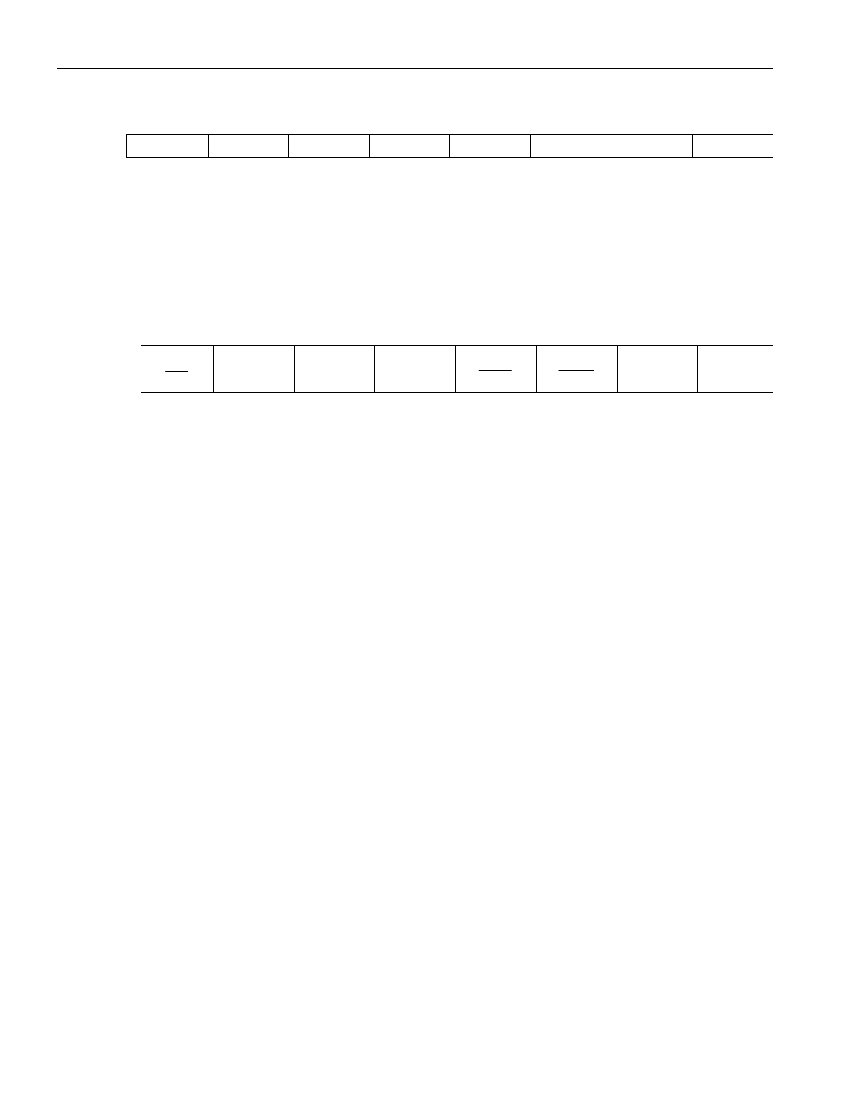
Slave Address Register 1 (SADDR1)
7 6 5 4 3 2 1 0
SFR AAh SADDR1.7 SADDR1.6 SADDR1.5 SADDR1.4 SADDR1.3 SADDR1.2 SADDR1.1 SADDR1.0
RW-0 RW-0 RW-0 RW-0 RW-0 RW-0 RW-0 RW-0
R = Unrestricted Read, W = Unrestricted Write, -n = Value after Reset
SADDR1.7–
SADDR1.0
Bits 7–0
Slave Address Register 1. This register is programmed with the given or broadcast
address assigned to serial port 1.
4.2.25
Port 3 (P3)
7 6 5 4 3 2 1 0
SFR B0h
P3.7
RD
P3.6
WR
P3.5
T1
P3.4
T0
P3.3
1
INT
P3.2
0
INT
P3.1
TXD0
P3.0
RXD0
RW-1
RW-1 RW-1 RW-1 RW-1 RW-1 RW-1 RW-1
R = Unrestricted Read, W = Unrestricted Write, -n = Value after Reset
P3.7–P3.0
Bits 7-0
General-Purpose I/O Port 3. This register functions as a general-purpose I/O port. In
addition, all the pins have an alternative function listed below. Each of the functions is
controlled by several other SFRs. The associated Port 3 latch bit must contain a logic one
before the pin can be used in its alternate function capacity.
RD
Bit 7
External Data Memory Read Strobe. This pin provides an active-low read strobe to an
external memory device.
WR
Bit 6
External Data Memory Write Strobe. This pin provides an active-low write strobe to an
external memory device.
T1
Bit 5
Timer/Counter External Input. A 1-to-0 transition on this pin will increment Timer 1.
T0
Bit 4
Counter External Input. A 1-to-0 transition on this pin will increment Timer 0.
INT1
Bit 3
External Interrupt 1. A falling edge/low level on this pin will cause an external interrupt
1 if enabled.
INT0
Bit 2
External Interrupt 0. A falling edge/low level on this pin will cause an external interrupt
0 if enabled.
TXD0
Bit 1
Serial Port 0 Transmit. This pin transmits the serial port 0 data in serial port modes 1, 2, 3
and emits the synchronizing clock in serial port mode 0.
RXD0
Bit 0
Serial Port 0 Receive. This pin receives the serial port 0 data in serial port modes 1, 2, 3
and is a bidirectional data transfer pin in serial port mode 0.