15 clock control (ckcon), Timer 0 lsb (tl0), Timer 1 lsb (tl1) – Maxim Integrated High-Speed Microcontroller User Manual
Page 31: Timer 0 msb (th0), Timer 1 msb (th1), Ckcon

High-Speed Microcontroller User’s Guide
Rev: 062210
31 of 176
4.2.15
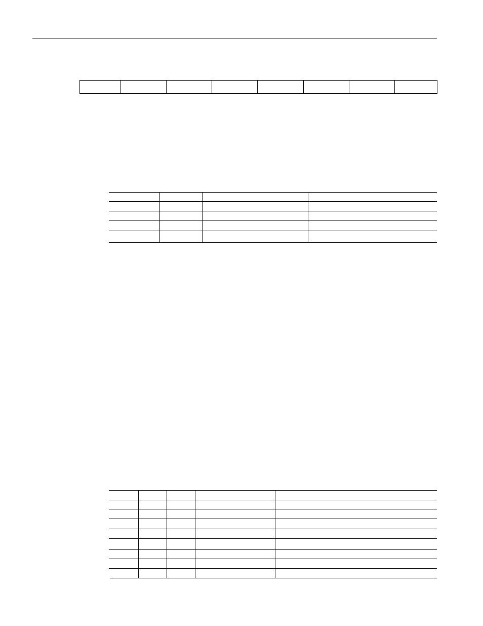
Clock Control (CKCON)
7 6 5 4 3 2 1 0
SFR 8Eh
WD1
WD0
T2M
T1M T0M MD2
MD1 MD0
RW-0 RW-0 RW-0 RW-0 RW-0 RW-0
RW-0 RW-1
R = Unrestricted Read, W = Unrestricted Write, -n = Value after Reset
Watchdog Timer Mode Select 1-0. These bits determine the watchdog timer timeout
period. The timer divides the crystal frequency by a programmable value as shown below.
The divider value is expressed in clock (crystal) cycles. The use of PMM1 or PMM2 will
further divide the clock cycle count by either 16 or 256, respectively. Note that the reset
timeout is 512 clocks longer than the interrupt, regardless of whether the interrupt is
enabled.
WD1 WD0
INTERRUPT
DIVIDER
RESET
DIVIDER
0 0
2
17
2
17
+ 512
0 1
2
20
2
20
+ 512
1 0
2
23
2
23
+ 512
1 1
2
26
2
26
+ 512
WD1, WD0
Bits 7, 6
T2M
Bit 5
Timer 2 Clock Select. This bit controls the division of the system clock that drives Timer
2. This bit has no effect when the timer is in baud-rate generator or clock output modes.
Clearing this bit to 0 maintains 80C32 compatibility. This bit has no effect on instruction
cycle timing.
0 = Timer 2 uses a divide-by-12 of the crystal frequency.
1 = Timer 2 uses a divide-by-4 of the crystal frequency.
T1M
Bit 4
Timer 1 Clock Select. This bit controls the division of the system clock that drives Timer
1. Clearing this bit to 0 maintains 80C32 compatibility. This bit has no effect on instruction
cycle timing.
0 = Timer 1 uses a divide-by-12 of the crystal frequency.
1 = Timer 1 uses a divide-by-4 of the crystal frequency.
T0M
Bit 3
Timer 0 Clock Select. This bit controls the division of the system clock that drives Timer
0. Clearing this bit to 0 maintains 80C32 compatibility. This bit has no effect on instruction
cycle timing. On the DS8xC520 and DS8xC530, Timer 0 will use a divide-by-4 of the
crystal frequency if Timer 0 is configured in mode 3, regardless of the setting of this bit.
This bit functions normally if Timer 0 is configured for any mode other than mode 3.
0 = Timer 0 uses a divide-by-12 of the crystal frequency.
1 = Timer 0 uses a divide-by-4 of the crystal frequency.
Stretch MOVX Select 2-0. These bits select the time by which external MOVX cycles are
to be stretched. This allows slower memory or peripherals to be accessed without using
ports or manual software intervention. The RD or WR strobe will be stretched by the
specified interval, which will be transparent to the software except for the increased time to
execute to MOVX instruction. All internal MOVX instructions on devices containing
MOVX SRAM are performed at the two-machine cycle rate.
MD2
MD1
MD0
STRETCH VALUE
MOVX DURATION
0
0
0
0
2 Machine Cycles
0
0
1
1
3 Machine Cycles (reset default)
0 1 0
2
4 Machine Cycles
0
1
1
3
5 Machine Cycles
1 0 0
4
6 Machine Cycles
1
0
1
5
7 Machine Cycles
1
1
0
6
8 Machine Cycles
MD2, MD1, MD0
Bits 2, 1, 0
1
1
1
7
9 Machine Cycles
