2 port 2, 1 general-purpose i/o, Parallel i/o – Maxim Integrated High-Speed Microcontroller User Manual
Page 113: General-purpose i/o, Multiplexed address/data bus ad0–ad7

High-Speed Microcontroller User’s Guide
Rev: 062210
113 of 176
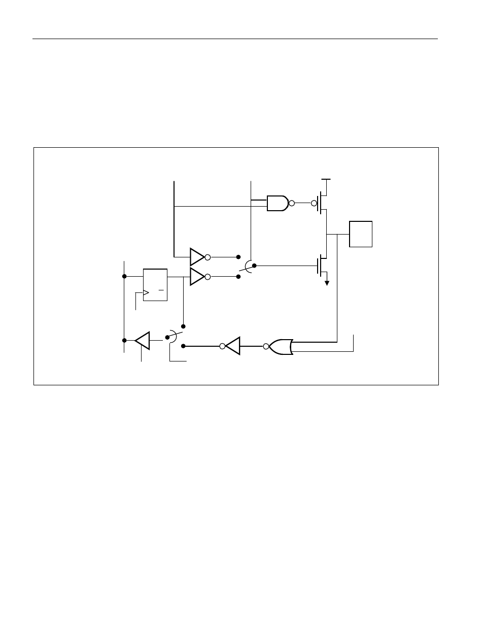
When used as an address bus, the AD0-7 pins will provide true drive capability for both logic levels. No
pullups are needed. In fact, pullups will degrade the memory interface timing. Members of the high-speed
microcontroller family employ a two-state drive system on AD0-7. That is, the pin is driven hard for a
period to allow the greatest possible setup or access time. Then the pin states are held in a weak latch
until forced to the next state or overwritten by an external device. This assures a smooth transition
between logic states and also allows a longer hold time. In general, the data is held (hold time) on AD0-7
until another device overwrites the bus. This latch effect is generally transparent to the user.
Figure 10-1. Port 0 Functional Circuitry
10.2 Port 2
10.2.1
General-Purpose I/O
Devices that have internal program memory have the ability to use Port 2 for a general-purpose I/O. Data
written
to the port latch serves to set both level and direction of the data on the pin. When used as an I/O
port, it has complementary outputs that will drive both high and low logic levels. More detail on the
functions of these pins is provided under the description of output and input functions in this section.
Even if internal memory is present, the use of Port 2 as general-purpose I/O pins is not recommended if
the device will be used to access external memory. This is because the state of the pins will be disturbed
during the memory access. It is still possible, however, to use the Port 2 latch to hold the upper address
byte for Register Indirect Addressing instructions.
ADDRESS\
DATA
EXTERNAL
ADDRESS
CONTROL
PORT
0.n
D
Q
Q
INTERNAL
DATA BUS
WRITE
ENABLE
READ
ENABLE
POWER
DOWN
READ
LATCH/PIN
VCC
