2 most significant address byte, a8–a15, 3 ports 1 and 3, General-purpose i/o – Maxim Integrated High-Speed Microcontroller User Manual
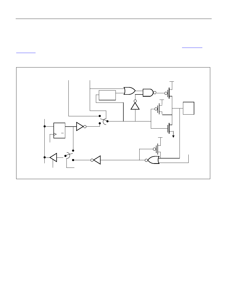
Page 114: Figure 10-1. port 0 functional circuitry
High-Speed Microcontroller User’s Guide
Rev: 062210
114 of 176
10.2.2
Most Significant Address Byte, A8–A15
When used to address expanded memory, Port 2 functions as the most significant byte of the address bus.
Port 2 must function as the address bus on ROMless devices. When serving as a bus, Port 2 will be driven
with strong drivers at all times except immediately after the rising edge of PSEN (
and
Figure 10-2. Port 2 Functional Circuitry
10.3 Ports 1 and 3
Ports 1 and 3 are general-purpose I/O ports with optional special functions associated with each pin.
Enabling the special function automatically converts the I/O pin to that function. To ensure proper
operation, each alternate function pin should be programmed to a logic 1. For example, enabling the
UART converts P3.0 and P3.1 to
the serial I/O functions.
The drive characteristics of these pins do not change when the pin is configured for general I/O or as the
special function associated with that pin. The exceptions are pins P3.6 and P3.7, which employ the
current-limited transition drivers described later when used as RD and WR signals. The drive
characteristics of Port 1 and Port 3 are the same as for Port 2 (non-bus mode). That is, the logic 0 is
created by a strong pulldown. The logic 1 is created by a strong transition pullup that changes to a weak
pullup.
Using one or more I/O pins of a port as special function pins will not affect the remaining port pins. An
extreme example is as follows. P3.6 has the alternate function of WR and P3.7 of RD. These strobes are
used for expanded data memory access. If a system used only the RD signal, then P3.6 would still be
available as an I/O port. This is not a practical suggestion, but it illustrates how the special functions are
independent.
ADDRESS
A8-A15
ADDRESS
CONTROL
D
Q
Q
INTERNAL
DATA BUS
WRITE
ENABLE
READ
ENABLE
READ
LATCH/PIN
PORT
0.n
VCC
DELAY
=2Tclk
POWER
DOWN
VCC
VCC