20 serial data buffer 0 (sbuf0), 21 port 2 (p2), Serial port 0 control (scon0) – Maxim Integrated High-Speed Microcontroller User Manual
Page 36: Sbuf0
High-Speed Microcontroller User’s Guide
Rev: 062210
36 of 176
TI_0
Bit 1
Transmitter Interrupt Flag. This bit indicates that data in the serial port 0 buffer has
been completely shifted out. In serial port mode 0, TI_0 is set at the end of the 8th data
bit. In all other modes, this bit is set at the end of the last data bit. This bit must be
manually cleared by software.
RI_0
Bit 0
Receiver Interrupt Flag. This bit indicates that a byte of data has been received in the
serial port 0 buffer. In serial port mode 0, RI_0 is set at the end of the 8th bit. In serial
port mode 1, RI_0 is set after the last sample of the incoming stop bit subject to the state
of SM2_0. In modes 2 and 3, RI_0 is set after the last sample of RB8_0. This bit must be
manually cleared by software.
4.2.20
Serial Data Buffer 0 (SBUF0)
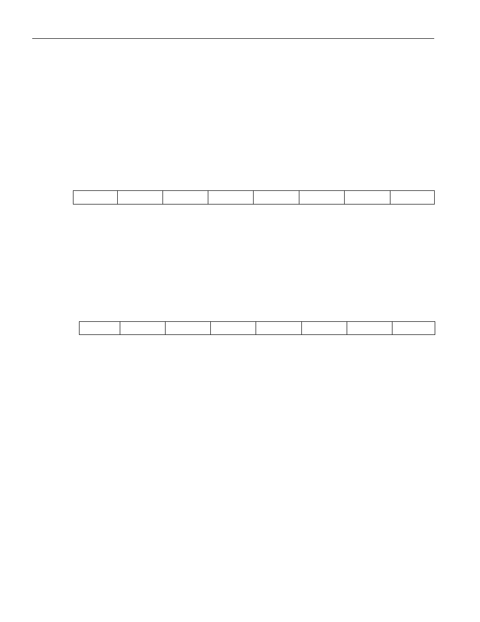
7 6 5 4 3 2 1 0
SFR 99h SBUF0.7
SBUF0.6
SBUF0.5
SBUF0.4 SBUF0.3 SBUF0.2 SBUF0.1 SBUF0.0
RW-0 RW-0 RW-0 RW-0 RW-0 RW-0 RW-0 RW-0
R = Unrestricted Read, W = Unrestricted Write, -n = Value after Reset
SBUF0.7–SBUF0.0
Bits 7–0
Serial Data Buffer 0. Data for serial port 0 is read from or written to this location. The
serial transmit and receive buffers are separate registers, but both are addressed at this
location.
4.2.21
Port 2 (P2)
7 6 5 4 3 2 1 0
SFR A0h
P2.7
P2.6
P2.5
P2.4 P2.3 P2.2
P2.1 P2.0
RW-1 RW-1 RW-1 RW-1 RW-1 RW-1
RW-1 RW-1
R = Unrestricted Read, W = Unrestricted Write, -n = Value after Reset
P2.7–P2.0
Bits 7–0
Port 2. This port functions as an address bus during external memory access, and as a
general-purpose I/O port on devices that incorporate internal program memory. During
external memory cycles, this port will contain the MSB of the address. The Port 2 latch
does not control general-purpose I/O pins on the DS80C310 and DS80C320, but is still
used to hold the address MSB during register-indirect data memory operations such as
MOVX A, @R1.