Epson S1D13705 User Manual
Page 69
Epson Research and Development
Page 63
Vancouver Design Center
Hardware Functional Specification
S1D13705
Issue Date: 02/02/01
X27A-A-001-10
REG[0Dh] bits 7-0
Screen 1 Start Address Bits [15:0]
REG[0Ch] bits 7-0
These bits determine the word address of the start of Screen 1 in Landscape modes or the
byte address of the start of Screen 1 in SwivelView modes.
Note
For SwivelView mode the most significant bit (bit 16) is located in REG[10h].
REG[0Fh] bits 7-0
Screen 2 Start Address Bits [15:0]
REG[0Eh] bits 7-0
These bits determine the word address of the start of Screen 2 in Landscape modes only
and has no effect in SwivelView modes.
bit 0
Screen 1 Start Address Bit 16
This bit is the most significant bit of Screen 1 Start Address for SwivelView mode. This
bit has no effect in Landscape mode.
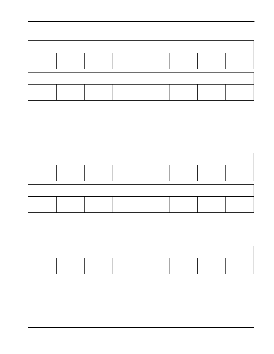
REG[0Ch] Screen 1 Start Address Register (LSB)
Address = 1FFECh
Read/Write
Screen 1 Start
Address
Bit 7
Screen 1 Start
Address
Bit 6
Screen 1 Start
Address
Bit 5
Screen 1 Start
Address
Bit 4
Screen 1 Start
Address
Bit 3
Screen 1 Start
Address
Bit 2
Screen 1 Start
Address
Bit 1
Screen 1 Start
Address
Bit 0
REG[0Dh] Screen 1 Start Address Register (MSB)
Address = 1FFEDh
Read/Write
Screen 1 Start
Address
Bit 15
Screen 1 Start
Address
Bit 14
Screen 1 Start
Address
Bit 13
Screen 1 Start
Address
Bit 12
Screen 1 Start
Address
Bit 11
Screen 1 Start
Address
Bit 10
Screen 1 Start
Address
Bit 9
Screen 1 Start
Address
Bit 8
REG[0Eh] Screen 2 Start Address Register (LSB)
Address = 1FFEEh
Read/Write
Screen 2 Start
Address
Bit 7
Screen 2 Start
Address
Bit 6
Screen 2 Start
Address
Bit 5
Screen 2 Start
Address
Bit 4
Screen 2 Start
Address
Bit 3
Screen 2 Start
Address
Bit 2
Screen 2 Start
Address
Bit 1
Screen 2 Start
Address
Bit 0
REG[0Fh] Screen 2 Start Address Register (MSB)
Address = 1FFEFh
Read/Write
Screen 2 Start
Address
Bit 15
Screen 2 Start
Address
Bit 14
Screen 2 Start
Address
Bit 13
Screen 2 Start
Address
Bit 12
Screen 2 Start
Address
Bit 11
Screen 2 Start
Address
Bit 10
Screen 2 Start
Address
Bit 9
Screen 2 Start
Address
Bit 8
REG[10h] Screen Start Address Overflow Register
Address = 1FFF0h
Read/Write
n/a
n/a
n/a
n/a
n/a
n/a
n/a
Screen 1 Start
Address
Bit 16